

1. Introduction
Integrated circuits fabricated on semiconductor substrates for large scale integration require multiple levels of metal interconnections to electrically interconnect the discrete layers of semiconductor devices on semiconductor chips. The different levels of interconnections are separated by various insulating or dielectric layers, which are etched via holes to connect a level of metal to the next level.
As the feature sizes shrink and the density of transistors on chips further increases, the electrical resistance and parasitic capacitance with back end of the line aluminum interconnections have become major factors which limit the circuit speed of high-performance integrated circuits (ICs).1-2) By decreasing the thickness of the insulating layers, the intra-level and inter-level capacitances between the metal lines increase since the capacitance is inversely proportional to the spacing between the lines. As the capacitance increases, the resistor-capacitor(RC) time delay increases. Increasing the RC time delay decreases the frequency response of the circuit and increases the signal propagation time through the circuit, thereby adversely affecting the circuit performance. Therefore, it is desirable to minimize the RC time constant. One approach to reduce these RC time delays is to use an insulating material having a lower dielectric constant k to reduce the capacitance between the metal lines. Low-k layers also help to prevent cross-talk between different metal layers and reduce device power consumption.
Among potential low-k materials, carbon-doped oxides or organosilicate glass (OSG, SiCO:H) have become the major candidates for potential applications beyond 130 nm device nodes. It has been shown that organic functional groups can dramatically decrease the dielectric constant by increasing the free volume of films.3-5) However, from the process integration point of view, this new group of low-k materials, which usually possess a low density and high porosity, has yet to demonstrate improved mechanical and thermal stabilities, including hardness, elastic modulus, and no delamination. Furthermore, as circuit densities continue to increase, the widths of these gaps decrease further, thereby increasing the gap aspect ratio, which is typically defined as the gap height divided by the gap width. As a result, filling these narrower gaps becomes more difficult, which can lead to unwanted voids and discontinuities in the insulating or gap-fill material.
We developed novel OSG films using dimethyl dimethoxy silane(DMDMOS) in CxHyOz as a carrier solvent in a flowable chemical vapor deposition(F-CVD) system. As a result, we obtained low-k films which have superior electrical and mechanical properties with super filling on inter metal dielectric(IMD) and shallow trench isolation (STI) patterns. In this paper, we report the basic film characteristics of low-k films fabricated by the F-CVD system and investigate the capability of gap-filling. A new process which leads to improved gap-filling properties is proposed and discussed.
2. Experimental Procedure
For the characterization of film properties, the OSG (organo silicate glass) films were deposited at 0 °C on non-patterned wafers by F-CVD. A main precursor, DMDMOS ((CH3)2Si(OCH3)2), and the additive (CxHyOz) as a carrier solvent were used in the experiments. The deposited wafers were baked at 400 °C for 1 min and cured in a UV flood at 430 °C for 110 sec under a nitrogen atmosphere. The film thickness and refractive index of the deposited films were measured by a reflectometer (Nano Metrix; NANO8300XSE) and/or ellipsometer (Woollam; Spectroscopic Ellipsometers M- 2000DI). The chemical bonding structures and compositions of the cured films were investigated by Fouriertransform infrared absorption spectra(FTIR) and Rutherford backscattering spectrometry-hydrogen forward scattering spectrometry(RBS-HFS). For electrical characterization, the relative permittivity, leakage current density, and breakdown field strength were measured at 1 MHz using a SSM Hg probe system. The errors of the capacitance and mercury electrode area measurements were less than 1 %. The densities of the low-k films were characterized by employing an X-ray reflectometer(XRR). The trench filling properties were determined by SEM.
3. Results and Discussion
FTIR measurements were performed to investigate the changes of the chemical bonding states of films fabricated under different curing conditions. Each film was sequentially baked in a hot chamber at 400 °C for 1 min under a nitrogen atmosphere followed by thermal annealing or UV curing. Fig. 1 shows the FTIR spectra of the (a) thermally baked film at 400 °C, (b) UV-cured (high pressure Hg lamp; lamp B) film, and (c) UV-cured (Xe lamp; lamp A) film prepared under a nitrogen atmosphere.
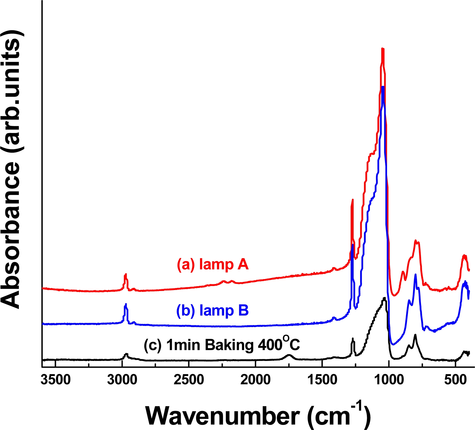
In Fig. 1(a), the Si-O main, -CH3, CH2-C, and CH3-Si peaks, which are typical low-k peaks, are observed at 1,070 cm−1, 2,930 cm−1, 1,750 cm−1, 1,265 cm−1, and 800 cm−1 in the thermally baked films. As compared to lamp A (a) and lamp B (b), an absorption peak around 2,200 cm−1 is observed(Fig. 1(c)). This peak originates from H2SiO2/2 units, which are formed via an exchange reaction under curing. Because of the difference of the backbonding coordination with three vs. two oxygen atoms, the Si-H stretching peak in the monohydride occurs at higher frequencies than that in the dihydride.6) However, after the lamp B cure, both Si-O and Si-H peaks related to the cage-like and H2SiO2/2 structure decrease or disappear. This indicates that the vibrational energies of the deposited films are lower in the lamp B-cured film than in the lamp A-cured film. Simply, the vibration energy of lamp A is higher than that of lamp B.
According to previous studies, the asymmetric Si-O stretching band appears at around 1,070 cm−1 for fully oxidized silicon. The peak of the asymmetric Si-O stretching vibration in the Si-Si-O structure appears in a lower energy region than that of the Si-O stretching vibration in the O-Si-O structure due to the back-bonding difference in 3-coordinated or 4-coordinated oxygen atoms. Moreover, the Si-O bending band at around 880 cm−1 is likely related to distortions due to the formation of Si-Si bonds, that is, a band from the (Si-)Si-O bond structure.6-10) The low vibrational energies of the lamp Bcured film imply that Si-Si-O bonds as well as Si-Si-O bonds exist in the lamp B-cured film. Therefore, we believe that the lamp-B cured film becomes a more Sirich film than the lamp A-cured film.
The film shrinkage and elastic modulus of the lamp A and lamp B films are shown in Fig. 2(a) and Fig. 2(b), respectively. The film shrinkage and elastic modulus are 26 % and 8.5 GPa for the lamp A film cured at 430 °C for 120 sec. In the case of lamp B, values of 25 % and 5.6 GPa after curing at 430 °C for 1,260 sec were obtained. The shrinkage rate and elastic modulus increase with increasing UV cure time for both lamp A and lamp B. However, the elastic modulus of the lamp B-cured film is much lower than that of the lamp A-cured film even with a long cure time. This result reveals that lamp A is more efficient for curing the OSG film.
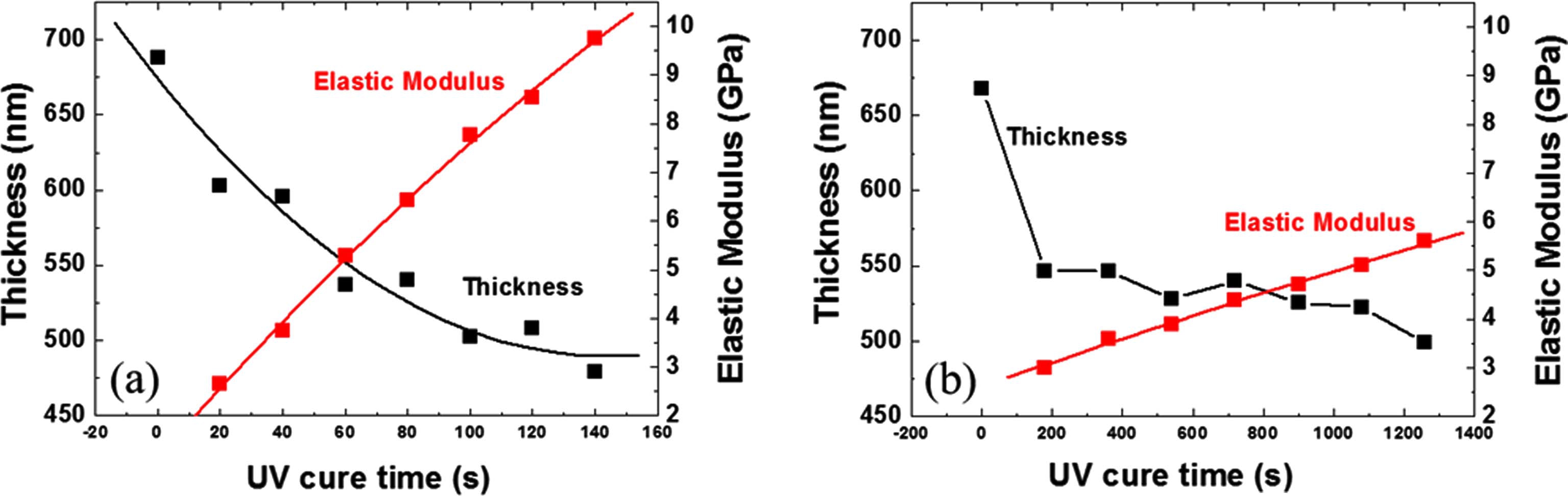
Fig. 2.
Shrinkage and elastic modulus of the deposited films with different UV cure times for (a) lamp A and (b) lamp B.
Fig. 3 shows the film stress and leakage current change as functions of the UV cure time. The electrical properties improved with increasing cure time. The leakage currents of the lamp A film cured for 120 sec and the lamp B film cured for 21 min are 3.8 × 10⁻⁹ and 5.8 × 10⁻⁹ at 2 MV/cm, respectively. Also, the film stress increased with increasing cure time. The electrical and mechanical properties of the different cured films are summarized in Table 1.
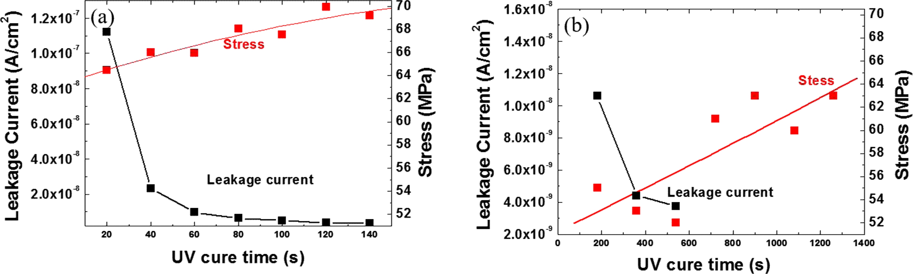
Fig. 3.
The film stress and leakage current as functions of the UV cure time for (a) lamp A and (b) lamp B.
Table 1.
The electrical and mechanical properties of the deposited films with different UV curing times.
In Table 1, the k value increases with cure time for both lamp A and lamp B. One of the interesting features is that the k value decreased after curing with lamp A for 40 sec and then, the k value increased. This implies that –OH and moisture still remain in the deposited OSG film. With further curing, –OH and moisture are removed from the deposited OSG film and then the film became dense. The density of the 120 sec UV-cured film cured by lamp A film was 1.1 g/cm3.
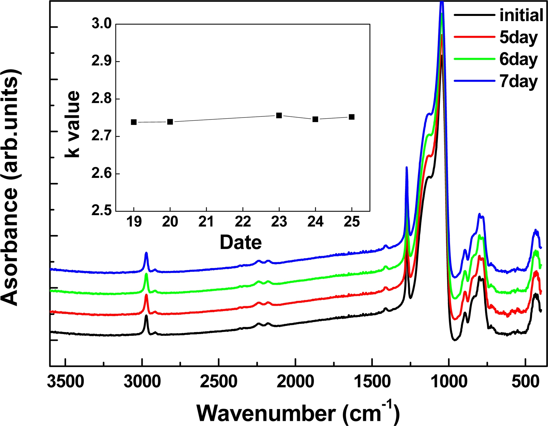
In order to determine the film stability, the UV-cured film(lamp A) was exposed for one week. Fig. 4 shows the FTIR transmittance spectra and k value change upon air exposure for one week. The FTIR transmittance and k value change results reveal that the deposited film is resistant to water molecule absorption.
The main precursor and additive composition deposited on trench patterns were investigated. This process can be divided into three different stages during deposition. First, the film grows in a conformal manner and secondly, it begins to grow much faster on the trench bottom of the features than on other parts of the substrates. Thirdly, after the completion of bottom up filling, the film growth rate abruptly slows down to the initial growth rate. As a result, the submicrometer features are filled in a bottom up fashion and after the completion of the bottom up filling, the surface becomes level.11)
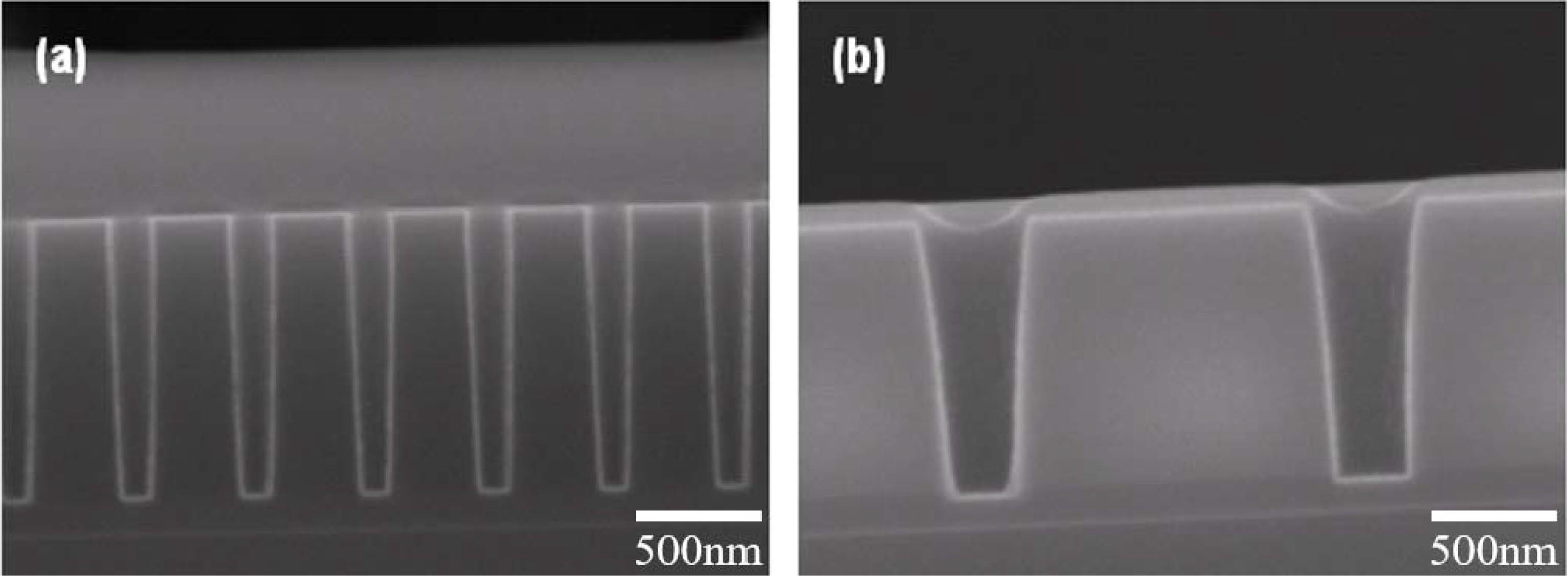
Fig. 5 shows the cross-sectional SEM photographs of the deposited OSG films on the patterns. As seen in this figure, the deposited OSG films are filled into the patterns without voids. In particular, we achieved the super-filling of defect-free high aspect ratio(> 7.5) features (Fig. 5(a)). Fig. 5(b) shows the bottom-up filling of the deposited films. Even after a very short deposition time, the deposits showed a transition from being subconformal to somewhat conformal at the side wall of the trench. Also, the trench structure is completely filled and the filling sequence of the trench is controlled because a longer deposition time is required to complete the bottom up filling of large trenches compared to small trenches. This represents a very promising result to realize gapfilling for IMD and STI by a CVD process.
4. Conclusions
The low-k film deposition process for gap-filling of submicrometer trenches using DMDMOS, (CH3)2Si(OCH3)2, and CxHyOz by plasma enhanced chemical vapor deposition is presented. We obtained low-k films which possess electrical stability and superior gap-filling properties on the trench patterns without voids or delamination. The newly developed technique, which is a low temperature process for a gap-filling of submicrometer features, will have a great impact on intermetallic dielectrics and shallow trench isolates for next generation microelectronic devices. Moreover, this bottom up gap-fill mode is expected to be universal for other chemical vapor deposition systems.
