

1. Introduction
Crystalline materials comprising a single layer of atoms are described as a two dimensional(2D) material.1,2) Since the discovery of these 2D materials back in 2004, their application rate has increased tremendously.3-7) Like the graphene which has potential application in flexible electronics, solar cells, biosensors, nanoelectromechanical system(NEMS) devices, etc. but lacks in semiconductor application due to zero bandgap.7-16) On the other hand, transition metal dichalcogenides(TMD) materials which are classified under 2D materials like Molybdenum disulphide(MoS2) is a good semiconductor at a single layer making its application in the field effect transistors (FET).17-20)
The physical and electrical properties of these 2D materials are usually studied using mechanically exfoliated 2D flakes on supporting SiO2/Si substrate due to their visibility using an optical microscope. However, without a substrate i.e. the 2D flake in a suspended form usually provides more accurate and reliable measurement. But to fabricate these suspended flakes is a troublesome.21-26) The contamination removal process at nanoscale is much difficult which provides inconsistent results with the fabricated 2D flake device. The contamination usually occurs with the poly-methyl methacrylate(PMMA) removal process using acetone or during the tailoring process of the 2D flake using focused ion beam(FIB) or E-beam lithography(EBL).27-33) Taking all these into account, there was a need to fabricate suspended 2D nanosheets onto a microelectromechanical system(MEMS) device. Also we used a dry transfer technique to transfer 2D flake onto the device to avoid the contamination between the 2D flake and device interface. As compared to other transfer methods, it provides clean, easy, less wrinkles way of transferring 2D flake onto the device but however this technique cannot be used for large scale 2D material transfer.34)
Here we report a residue free standard procedure to fabricate suspended 2D flakes onto a MEMS device. Further the tailoring of these suspended 2D nanosheets can be done by FIB, focused electron beam(FEB) or helium ion microscopy(HIM) milling to study the in-situ nanomechanics using transmission electron microscope (TEM).
2. Experimental Details
2 cm× 2 cm marked silicon(Wafer mart, South Korea) substrate is initially cleaned in acetone(high purity grade, Duksan Chemicals, South Korea), then into isopropanol (high purity grade, Duksan Chemicals, South Korea) and distilled water to get rid of any residues by ultrasonication. Then it is covered with Polystyrene sulfonic (PSS; Sigma Aldrich) and PMMA(Duksan Pure Chemicals) polymer layer to proceed with the dry transfer process as shown in Fig. 1. 2D flakes of graphene and MoS2 were obtained by mechanical exfoliation of bulk material(HQ graphene, high grade) with a strip of blue nitto tape(Fig. 1). The strip is folded several times in different angles with itself until the bulk material is spread over a defined area of the tape. From the used tape some of the cleaved bulk flakes are transferred onto a new tape which is folded again several times with itself to cleave the 2D flake further more. This step can be repeated depending on the density of bulk material on the tape. The area of the last tape, also referred to as transfer tape in this work, which is covered by very thin layers of bulk 2D flake is then pressed onto the surface of the substrate before the tape is lifted off again very slowly.3,35,36) These substrates containing 2D flakes and their bulk were then scanned with an optical microscopy to locate the area of interest of 2D flake with 100x objective lens(Olympus BX51), the images were captured by CCD camera(Canon EOS- 1D X), with the help of EOS utility software to store the images in the computer in auto exposures and auto white modes of 5184 × 3456 pixels.
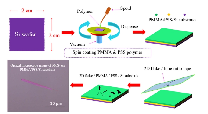
Fig. 1
Process to obtain mechanically exfoliated 2D flakes with different number of layers. Obtained optical microscope image of MoS2 flake(with 3 number of layers) on the PMMA/PSS/Si substrate.
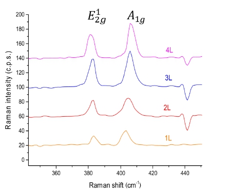
Fig. 2
Comparison of the difference in intensity of E 1 2g band peak and A1g band peak on SiO2/Si substrates in Raman spectra as a function of number of layers for 532 nm excitation; E 1 2g band ranges from 382-385 cm−1 and A1g band ranges from 402-406 cm−1.
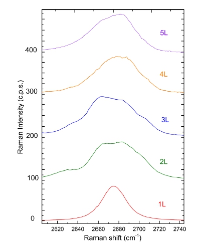
The 2D flakes(area of interest) must always be placed at the center of the image to get consistent results. In order to identify the number of layers, Raman spectroscopy (Thermo Scientific DXR) with 532 nm and full range grating was used and the data was saved in omnic software on the computer. The laser beam is focused onto the 2D flake samples by a 50x microscope objective lens and the images were detected using CCD detector. The Raman result indicates the E12g band and the A1g band shape of a peak for MoS2 whose difference varies with number of layers(Fig. 2).37) While in the case of graphene it is the peak shape change in the 2D band of Raman spectra that describes the number of layers(Fig. 3).38-40) As the graphene layers increase(in Fig. 3), the branching of the electronic bands and the phonon dispersion at the K point occurs which are responsible to the shape change of 2D peak in Raman spectra.40)
3. Results and Discussion
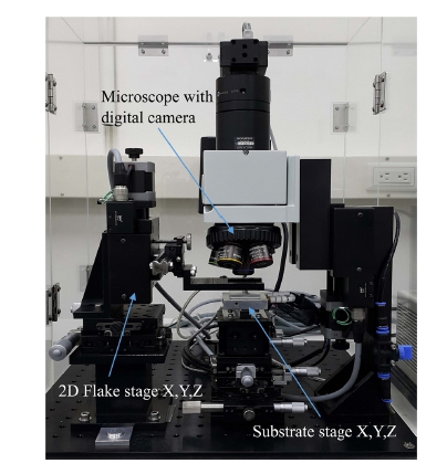
The device is fabricated using a dry transfer process (Fig. 4) i.e. the surface of the 2D flake is transferred to another substrate without any chemicals in contact in between them. After identifying the number of layers of the 2D flake, the substrate with 2D flake is then covered with thermal release tape(TRT) with a hole at the center as shown in Fig. 4. The TRT acts as a supporting layer to the 2D flake on PMMA to transfer to another substrate. Then the whole structure is placed in water to separate the Si substrate from 2D flake on PMMA. After separation the TRT with suspended 2D flake on PMMA was dried thoroughly using kimtech wipers and desiccator( 1 day recommended). The 2D flake along with PMMA was transferred on push-to-pull(ptp) device using the transfer system as shown in the Fig. 5 to align the position of the 2D flake on the ptp device.27,41,42)
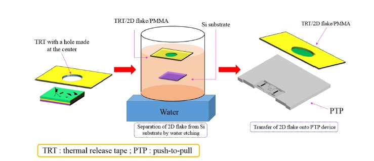
Fig. 4
Dry transfer process of the 2D flake onto the target substrate to suspend with the help of PMMA supporting layer. The target substrate is push to pull(PTP) device for tensile testing in TEM.
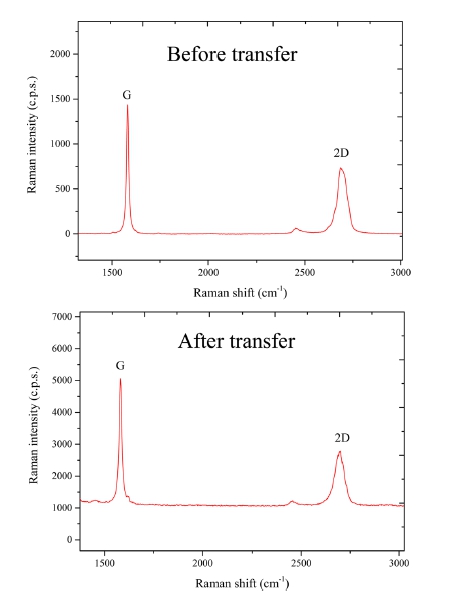
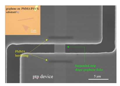
The flake was then clamped to the device using Ebeam lithography(EBL) technique as shown in Fig. 6.43) Clamping is necessary to avoid any slack formation in the transferred 2D flake on the device. Here the PMMA surrounding the 2D flake is hardened using EBL so that the flake is firmly attached to ptp. The pattering is done in a rectangle shape of size 6 μm × 2 μm with a high beam dose of 12000 μC/cm2. The reason behind using PMMA as clamping is to reuse the ptp device rather than having metal clamping using FIB. Later the ptp with 2D flake and PMMA was transferred to N-Methyl-2-pyrrolidone (NMP) solution to remove the PMMA from the device. However the hardened PMMA during the EBL process is not removed in NMP solution. The same was confirmed by taking SEM images before and after PMMA removal. During the lift of from the NMP solution the suspended 2D flake was broken due to the surface tension. Hence, it was further transferred to IPA solution and then transferred to liquid CO2 in critical point dryer(CPD) chamber to reduce the surface tension effect. Also while transferring the ptp with 2D flake to various solution, it must always be kept in liquid medium. The unwanted flake suspended on the spring part of the ptp device was removed using focus ion beam(FIB) milling process(Fig. 6). The suspended 2D flake was again characterized by Raman spectra to identify the damaged occurred in the flake after transfer process. It is compared with the Raman spectra obtained from the 2D flake before the transfer process. Fig. 7 shows the comparison of Raman spectra of strip shape graphene flake before and after transfer process. The 2D band peak(in Fig. 7) in the Raman spectra verifies that the flake is three layer graphene as per the identification of number of graphene layers mentioned in Fig. 3. It can be seen that the 2D peak shape is slightly changed due to the contamination of acetone while removing the PMMA from the dry transfer process. Also another possibility is that the PMMA residue still remained on the suspended flake.
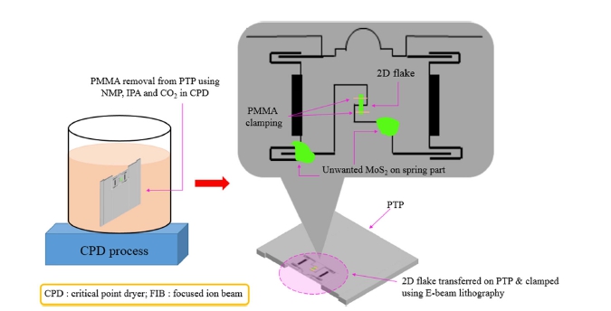
Fig. 6
PMMA removal process using the NMP and CPD chamber to suspend the 2D flake without any external disturbances.
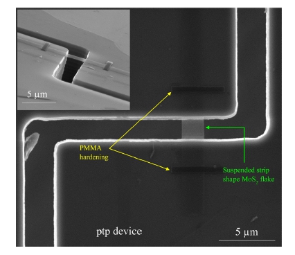
After PMMA removal process clean, residue free suspended 2D flake with hardened PMMA clamping on the ptp device was obtained. Fig. 8 shows the scanning electron microscope(SEM) image of the MoS2 flake with three number of layers which was successfully transferred without any contamination and folding of side edges. Also in the corner of Fig. 8, the tilt image of the MoS2 flake shows that there is no slack due to clamping it with PMMA. Similar result was obtained for graphene as shown in Fig. 9 for three number of layers. This process can be further used for other 2D flakes but is applicable to small devices only. It cannot be used for large scale 2D materials.
4. Conclusions
Mechanically exfoliated strip shape 2D flakes of graphene and MoS2 were prepared on PMMA/PSS/Si substrate. Using Raman spectra, the number of layers were identified and then transferred onto the ptp device using dry transfer method. Our proposed dry transfer process using PMMA for the transfer of 2D nanosheet onto the target substrate is a clean, residue free method. The 2D flake was clamped to the device using e-beam lithography to avoid slack formation. The PMMA after transfer process is removed using NMP, IPA and CPD process. Thus making it more reliable and controllable way of a fabricating micrometer-sized suspended 2D nanosheet.
