

1. Introduction
Graphene, a 2-dimensional(2-D) hexagonal lattice of carbon atoms discovered by Andre Geim and Kostya Novoselov has obtained much attention for the past 12 years in the scientific community due to its recognizable properties and potentials in nanotechnology and material applications.1,2) It is the basic building block for carbon nanomaterials like zero dimensional (0D) fullerenes, one dimensional (1D) carbon nanotubes and 2D nanographite sheets. Considering the electronic band structure of graphene, the conduction band touches the valence band at two points (K and K') in the Brillouin zone. Also in the surroundings of these points, the electron energy has a linear relationship with the wave vector, E = hkvf. Hence, electrons possessed by an ideal graphene acts like massless Dirac Fermions.1) The unique properties of graphene make it a promising candidate for fundamental study as well as for potential device applications. The charge carriers in graphene can be tuned continuously between electrons and holes in concentrations n as large as 1012/cm2. Graphene mobility is ~120000 cm2/(V.s) at room temperature which is the highest than any known semiconductor. Also, the graphene application in spintronics received a lot of importance as the spin relaxation length of ~2 μm has been observed in graphene that suggests a promising future for the graphene spintronics. Many other applications of graphene have also been reported.3)
Although monolayer graphene possesses most desirable properties for device applications, multilayer graphene is just as important due to advantages it has over monolayer graphene.4,5) For instance, the bilayer graphene as well as the trilayer graphene have useful characteristics based on their stacking sequence, interlaying spacing and relative twist.6) Also, the former has a wide tunable bandgap7) and the latter is a semimetal with a resistivity that decreases under increasing electric field.8) Not only effect of stacking order,9) interlayer coupling and relative layer orientation on several properties were observed to vary with the number of graphene layers but also various reports depicted thermal conductivity,10) electrical properties,11) friction12) and stiffness13) depends on the number of graphene layers.
2. Experimental Details
Graphene was obtained by exfoliation of graphite (HOPG, low grade) with a strip of scotch tape. The strip is folded several times in different angles with itself until the graphite is spread over a defined area of the tape. From the used tape some of the cleaved graphitic materials is transferred onto a new tape which is folded again several times with itself to cleave the graphite further more. This step can be repeated depending on the density of graphite on the tape. The area of the last tape, also referred to as transfer tape in this work, which is covered by very thin layers of graphite is then pressed onto the surface of the substrate before the tape is lifted off again very slowly. The substrate silicon covered by wet thermal oxidation of 3000A layer(wafer mart, South Korea) is initially cleaned in acetone(high purity grade, Duksan Chemicals, South Korea), then into isopropanol (high purity grade, Duksan Chemicals, South Korea) and distilled water(prepared in laboratory using Barnstead glass still) to get rid of any residues by ultra-sonication. These substrates containing graphene and graphite were then scanned with optical microscopy to calculate RGB values with 100x objective lens(Olympus BX51), the images were captured by CCD camera(Canon EOS-1D X), with the help of NIS software to store the images in the computer in auto exposures and auto white modes of 5184 × 3456 pixels. The graphene flakes(area of interest) must always be placed at the center of the image to get consistent results.4) The RGB values were calculated using the ImageJ(IJ 1.46r) software and Microscoft Excel 2013. In order to identify the number of layers Raman Spectroscopy( Thermo Scientific DXR Raman Microscope) with 532 nm and full range grating was used and the data was saved in omnic software on the computer. The laser beam is focused onto the graphene samples by a 50x microscope objective lens and the images were detected using CCD detector. The Raman result indicates the G band and the 2D band shape of a peak for graphene which varies with number of layers(as shown in Fig. 1). The optical images and the Raman spectroscopy data are then correlated in a graph format using the Origin software.
3. Results and Discussion
To identify the number of layers in multilayer graphene, exfoliated by mechanical cleaving, many methods have been proposed, e.g. the optical microscope image, Raman spectroscopy, atomic force microscopy, transmission electron microscopy. The transmission electron microscopy (TEM) is a technique in which a beam of electrons is transmitted through the graphene sample to interact with it as it passes through and accordingly the image is formed. But TEM needs graphene sheet samples suspended to ensure that optical absorption is solely due to graphene and later after characterization it will no longer be useable.14)
Atomic-force microscopy(AFM) is a very-high-resolution type of scanning probe microscopy(SPM) with demonstrated resolution on the order of fractions of a nanometer. The machine gathers information by “feeling” or “touching” the surface with the help of a mechanical probe. There are Piezoelectric elements which promote tiny but accurate and precise movements on scanning the area of interest.15) It is a very powerful and adaptable microscopy technique for the characterization of nanomaterials. It is used for various surface measurements and can provide a very high resolution topographic image.14) The AFM is one of the first techniques used to analyze graphene and other 2D materials but it also claims to have some drawbacks. The single layer graphene observed under the AFM on oxidized wafers typically displayed the thickness to be 0.8~1.2 nm thick adding layer on top of it more than the expected 0.35 nm thickness, which is the actual thickness due to the van der Waals interlayer distance. According to Caterina et al, folded graphene or rough substrate might be the reasons for this additional height measurement but the reason is still unclear. In tapping mode AFM, graphene thickness measurement undergo from certain anomalies evoked by improperly chosen free amplitude values for the cantilever.16) Also AFM is time consuming and confined in lateral scanning so that it can be used as a primary method to determine the thickness of graphene.17)
Raman spectroscopy is another tool to spot out the number of layers in multilayer graphene. It avails monochromatic laser to connect with the molecular vibrational modes and the phonons in a sample, shifting the laser energy down(Stokes) or up(anti-Stokes) through inelastic scattering. This energy shift generates two main peaks or the band in Raman spectrum: G(1580 cm−1), a primary in-plane vibrational mode and 2D(2690 cm−1) a second order in plane vibration. The area cited are from a 532 nm excitation laser. Due to the added forces from the interactions between layers of AB-stacked graphene, the 2D peak(band) shape change will occur as the number of layers of graphene increases into a wider, shorter higher frequency peak. Hence the number of layers can be derived from the ratio of peak(band) intensities, IG/I2D or from the shape and position of these peaks. But the method is not full proof, doping and defects mostly complicates the spectra18) making it challenging to differentiate the number of layers in multilayer graphene. Also stack faults is a reason to avoid Raman spectroscopy as reported in.19) Hence a close and meticulous examination of the shape of the 2D peak is required in order to find the actual number of layers using Raman Spectroscopy data.19)
Relative luminance(RL)4) is the relative brightness of any point in a color-space, normalized to 0 for the darkest black and 1 for the brightest white. For a certain point(or pixel) in a color image encoded in the standard RGB(sRGB) color-space, the RL can be computed based on the value of the sRGB components through the equation RL = 0.2126R + 0.7152G + 0.0722B.4,20) Most optical microscopes adopt episcopic illumination, which means that the light received by a camera is the light reflected from the specimen. In the case of graphene on SiO2/Si substrate, the amount of reflected light decreases as it passes through the graphene layer or layers because it is not perfectly transparent.21) This results in a noticeable difference between the RL values of the regions where graphene is present(RLG) and those where graphene is absent(RLS) and this difference(ΔRLGS = RLS − RLG) can be used to determine the thickness of the graphene flake in question. To enhance accuracy, the regions of interest to be compared should be made large enough. In addition, raw image data should be used instead of the typically compressed and processed image produced by the image capture software. As reported in,4) this method was verified using AFM method but we cannot trust this result due to the disadvantages of AFM method mentioned above. Hence single method cannot provide the utmost accurate result. In order to get reliable results, a combination of these methods must be used to determine the number of layers. Thus our work focus on comparison of the data of two existing methods to get a linear relationship. A combination of three methods is also possible but it is time consuming.
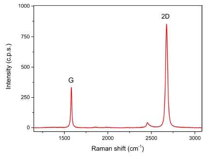
The Raman spectroscopy measurement of a multilayer graphene on wet oxidative silicon substrate provides useful information on the defects(D-band), in-plane vibration of sp2 carbon atoms(G-band) and also the stacking order (2D-band).3) Fig. 1 depicts the stokes phonon energy shift caused by laser excitation, thus producing the G-band and 2D-band in the graph of monolayer graphene sample.22) The single and sharp second order Raman 2D-band has been widely used as a simple and efficient way to confirm the presence of monolayer graphene(SLG). The 2D-band of multilayer graphene is formed by the accumulation of multiple peaks which shows a wider and shorter peak as compared to monolayer graphene. This happens because the electronic band structure splits in the multilayer material thus making it easy to differentiate in various number of layers of graphene. Fig. 2 shows the 2D-band shape change as the number of layers increases(up to 5 layers in the present study). To verify the same, the result is compared with the AFM data and the RGB values to get a linear relationship and making the data more accurate and reliable. Fig. 3 shows the optical microscopy image and the AFM scanned image along with the Raman spectroscopy data for the different locations as shown in the image. We observed that the 2D-band shape change is more accurate and hence it is considered as the base for the number of layers. Hence the x-axis is considered as number of layers based on the 2D-band shape change data in all the mentioned graphs. Fig. 4 and Fig. 6 provides the comparison of RGB values, intensity ratios of G band peak to the 2D band peak and the 2D band shape change(number of layers) with a linear relationship in Fig. 4. Also the comparison of AFM measurement data with number of layers as shown in Fig. 5 is not a linear one making it unfaithful to determine the number of layers in multilayer graphene.
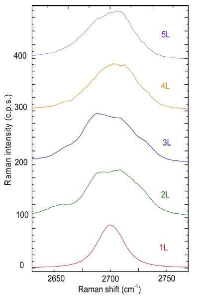
Fig. 2
Comparison of the 2D peak shape in Raman spectra as a function of number of layers for 532 nm excitation; 2D band ranges from 2674-2709 cm−1.
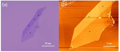
Fig. 3
Exfoliated graphene sample with different number of layers measured by (a) optical microscopy, (b) atomic force microscopy and Raman spectroscopy at different points marked with black color.
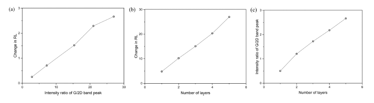
Fig. 4
Comparison of the methods used to check the consistency in any two methods to easily determine the number of layers in graphene. Correlations of (a) change in relative luminance in optical microscope image with Intensity ratio of G/2D band peak in Raman Spectroscopy, (b) change in relative luminance in optical microscope image with 2D band peak shape change in Raman spectroscopy and (c) intensity ratio of G/2D band peak with 2D band peak shape change in Raman spectroscopy. (From a selected data).
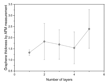
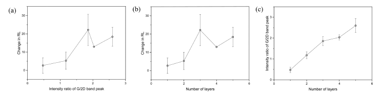
Fig. 6
Comparison of the methods used to check the consistency in any two methods to easily determine the number of layers in graphene. Correlations of (a) change in relative luminance in optical microscope image with intensity ratio of G/2D band peak in Raman spectroscopy, (b) change in relative luminance in optical microscope image with 2D band peak shape change in Raman spectroscopy and (c) intensity ratio of G/2D band peak with 2D band peak shape change in Raman spectroscopy.
4. Conclusions
The comparison of two existing methods was successfully applied to pristine graphene and the linear curve was obtained making it more reliable and easy to use in order to find the number of layers in multilayered graphene. The analysis concluded to use the comparison of number of layer(from 2D-band shape change) with the intensity ratio of G to 2D band and provides a consistent result. Comparison of existing three methods would be a time consuming process.
