

1. Introduction
Dynamic random-access memory (DRAM) is a volatile memory used for storing and retrieving information. It consists of one switching transistor and one capacitor, which stores charges. To increase the capacitance of this capacitor, the electrode area should be larger, the thickness of the dielectric layer should be thinner, and the dielectric constant (k) should be higher. However, it is difficult to increase the electrode area due to the scaling of DRAM. Reducing the thickness of dielectrics can lead to an increment of leakage current due to direct tunneling.1) Therefore, it is necessary to utilize materials with a high dielectric constant along with minimization of leakage current.2)
TiO2 has a very high dielectric constant, ranging from 30~75 in the anatase phase and 90~170 in the rutile phase, making it suitable for use as the dielectric layer in capacitors.3) However, when the dielectric constant is high, there is a tendency to separate atomic nuclei and charges in the insulating layer when a voltage is applied, leading to increased leakage current. TiO2 has a low energy bandgap of 3.0 eV, causing a decrease in band offsets and showing a tendency for electron leakage from the presence of oxygen vacancies due to the weak binding energy of Ti-O bonding.4) Furthermore, the conduction band offset (CBO) difference between TiO2 and the Si substrate is only 0.1 eV, further worsening the increased leakage current issue.5,6) Such an increased leakage current can reduce the operational lifespan of DRAM devices, leading to decreased device performance. Due to these characteristics, TiO2 has limitations as a dielectric material in the capacitor despite its high dielectric constant. This study aims to mitigate the leakage current characteristics of TiO2 to achieve meaningful performance enhancement as a dielectric layer in the capacitor. Fig. 1 shows a schematic of the DRAM capacitor and its leakage current issue due to direct tunneling.

Plasma-enhanced atomic layer deposition (PEALD) is a technology that allows precise control of atomic-level film thickness. It can operate at relatively low temperatures, minimizing defects and structural changes caused by heat. Additionally, plasma activation reduces surface defects, enabling the formation of a thin film with high density and uniformity.7) Therefore, by using PEALD to deposit TiO2, the defect density of TiO2 is expected to decrease, resulting in reduced leakage current. In this study, TiCl4 and O2 plasma were used as Ti precursor and reactant gas, respectively. Chiappim et al.8) describe that when depositing TiO2 using TiCl4 precursor, it has some limitations when used together with water as a hydrogen-based reaction precursor. According to it, when the halide precursor TiCl4 reacts with hydrogen-based precursor, it can produce gaseous byproducts with their strong corrosive nature. These corrosive byproducts can potentially corrode reactor components or even the grown films. Additionally, as a new alternative oxidant source in ALD, oxygen plasma is widely used, and when depositing TiO2 via PEALD using TiCl4, oxygen plasma can prevent water combustion or the formation of corrosive byproducts during the process.8,9)
Leakage current can be mitigated depending on the material used for the bottom electrode. Previously, poly-Si substrates were primarily used, but they have an unwanted SiO2 layer at the surface with low dielectric properties, which results in poor interfacial characteristics with high-k materials. The selection of suitable bottom electrode materials to replace traditional substrate materials is necessary, and they should be stable in a high-temperature oxygen atmosphere and maintain excellent conductivity even after oxidation. Oxygen in the dielectric layer oxidizes the electrode, generating oxygen vacancies and excessive electrons, deteriorating the interface characteristic qualities of the electrode and lowering electron mobility. Additionally, the substrate materials should have a high work function. High work function helps form a barrier with the dielectric layer, therefore, those materials increase Schottky barrier height and thus reduce leakage current. High work function materials include transition metal nitrides and precious metals, among others.10) Transition metal nitrides such as TiN and precious metals such as Pt and Ru can be used for bottom electrode materials. Pt has high oxidation resistance and very high melting temperature, so having excellent thermal stability. Pt also possesses a high work function of around 5.6 eV, which is sufficient for increasing barrier height compared to TiN. Ru also has a high work function of around 4.7 eV and low resistivity of about 7 µΩ ‧ cm. It exhibits excellent thermal and chemical stability. One of the oxides of Ruthenium, RuO2, possesses a higher work function of around 5.1 eV and has a rutile structure, which offers excellent structural compatibility with rutile-phase TiO2. According to Kim et al.,11) when TiO2 was deposited using thermal ALD with O3 reactant at 250 °C, the Ru substrate was strongly oxidized and exhibited higher structural compatibility with rutile TiO2 compared to H2O being used. It stated that it is crucial to use a very high concentration of O3, about 400 g/m2 to form the rutile phase for high dielectric constant.12) In our study, we aim to present leakage current and dielectric properties controlled through another method of heat treatment of the Ru substrate to first form RuO2 and form rutile TiO2 using PEALD with O2 plasma. Hollow cathode plasma was mainly employed as a plasma source, which could enhance the crystallinity of the film at low temperatures.13) Besides these characteristics, RuO2 has a resistivity of about 30 µΩ ‧ cm, providing superior conductivity to other oxide layers.10,14,15) When RuO2 is formed as an intermediate layer between the Ru substrate and TiO2 thin film, it can prevent leakage current due to electrons flowing from the substrate to the TiO2 layer. Ru films exhibit stability against oxidation up to 400 °C. Oxidation at 500 °C results in the formation of a mixed phase containing Ru and RuO2, while at 600 °C, a RuO2 layer is formed by rapid thermal annealing (RTA).16,17)
In this study, PEALD was used to deposit the TiO2 layer on the bottom electrodes including TiN and Pt, and pre-oxidized Ru substrates at 500 and 600 °C.11,18) Pt substrate was used to investigate the leakage current characteristics concerning the increase in work function, with TiN substrates serving as a reference group. Additionally, the formation of RuO2 on Ru substrates was utilized to examine the leakage current characteristics related to the intermediate layer and its structural compatibility with rutile TiO2. The change in dielectric constant and equivalent oxide thickness (EOT) of PEALD-grown TiO2 thin films were studied according to the bottom electrode materials.
2. Experimental Procedure
For this study, 10 kinds of devices were fabricated with variations in the bottom electrode (TiN, Pt, and Ru on SiO2/Si), TiO2 film thickness, and heat treatment conditions of Ru to compare the structural, chemical, and electrical properties of TiO2 thin films. Especially for Ru, three types of substrates with pre-heating were prepared to examine the structural compatibility, such as lattice mismatch between rutile TiO2 and RuO2. Untreated Ru and pre-heated Ru to 500 and 600 °C by RTA process were used. The pre-heating process was conducted in an O2 gas ambient, with temperatures at 500 and 600 °C. The heating rate was maintained at 100 °C/s for 60 s. TiO2 was deposited at 313 °C via the PEALD process. Titanium tetrachloride (TiCl4) and O2 plasma were used respectively as precursors and reactants in TiO2 thin film deposition. Fig. 2 shows the process sequence of PEALD. The recipe consisted of one cycle of deposition: TiCl4 dosing (1 s) - N2 purge (60 s) - O2 plasma (15 s) - N2 purge (60 s). TiO2 thin films were deposited for 200 and 400 cycles. The Pt, as the top electrode, was deposited using a sputtering system. The sputtering process was carried out with 3 min of pre-sputtering and 22 min of the main process. The thickness of TiO2 was measured using an ellipsometer (FS-1 multi-wavelength ellipsometer, Film-Sense), and the thickness and surface morphology was confirmed by field-emission scanning electron microscopy (FE-SEM, JSM-6700F, JEOL Ltd.). Ti area density was measured through X-ray fluorescence spectroscopy (XRF, US/ARL QUANTX, Thermoscientific). The crystallinity was confirmed using X-ray diffraction (XRD, Dmax 2500/PC, Rigaku). From the results of XRD analysis, average crystalline sizes were calculated by Scherrer’s equation. Atomic force microscopy (AFM, NX10, Park Systems) was utilized to analyze the surface roughness characteristics of the thin films after TiO2 deposition. The electrical properties, including the I-V (current-voltage) and C-V (capacitance-voltage) characteristics of devices, were measured using parameter analyzers (HP-4155 and Keithley 4200). The dielectric constant and EOT were calculated by the values from the capacitance. All the electrical measurement was performed at room temperature (25 °C).

3. Results and Discussion
TiO2 thin film was deposited according to PEALD cycles. Fig. 3(a) shows the thickness monitored by an ellipsometer. The thickness of 200-cycle deposited TiO2 thin film is about 21.67 nm, and that of 400-cycle deposited film is about 46.55 nm. The thickness monitoring was performed by using Si substrates. The growth-per-cycle acquired from the slope of linear fitting was 0.12 nm/cycle. Fig. 3(b) shows Ti area density as a function of ALD cycle measured from an XRF analysis. As the number of ALD cycles increases, Ti area density increases linearly. So, it can also prove that the thickness of TiO2 was well controlled by the ALD process. 10 kinds of capacitors were fabricated and named as follows: T200 (T400) and P200 (P400) denote the 200- (400-) cycle deposited TiO2 on TiN and Pt bottom electrodes, respectively. R(0)200, R(500)200, and R(600)200 represent 200-cycle deposited TiO2 on unheated Ru, and pre-heated Ru at 500 and 600 °C, respectively. R(0)400, R(500)400, and R(600)400 are the same except for 400-cycle deposited TiO2 on them.

Fig. 4 is the FE-SEM image of the T400 sample. Uniformly deposited TiO2 of about 47 nm on the TiN substrate is shown. The TiO2 thin film can be grown into various phases by many factors including the process temperature and time of ALD, the precursor and the usage of plasma, and the thickness of film.9,19,20,21) It turned out that the phase of TiO2 was rutile in all samples. High density and power of plasma generated by hollow cathode could enhance the crystallinity of the as-grown film irrespective of the substrate.13)Fig. 5(a, b) show the XRD patterns of 200-cycle and 400-cycle deposited TiO2 samples on the various substrates. The (110) peak is located at 2θ of 27.5° and the (101), (200), (111), (211), and (220) peaks are observed at 36.1°, 39.2°, 41.3°, 54.3°, and 56.7°. The intensities of TiO2-related peaks are greater in 400-cycle deposited samples than those in 200-cycle deposited samples. In 400-cycle deposited samples, 2 times thicker films were grown and TiO2 layer was more crystallized because the ALD process time was twice longer. Among the samples, RuO2 was formed in R(600)200 and R(600)400. The intensities of RuO2-related peaks at 28.1°, 35.2°, and 54.3°, which correspond to (110), (101), and (211), respectively, are also greater in 400-cycle deposited samples. It is because 400-cycle deposited samples were exposed to more heat and plasma energy in longer ALD process, therefore, RuO2 on Ru was more easily crystallized with the influence of the epitaxial growth of TiO2. Table 1 shows the average crystalline size of (110) and (211) planes of all samples. These values were calculated by Scherrer’s equation for two planes. The primary peak (110) has more influence on capacitance than the secondary peak (211). The dielectric constant of rutile TiO2 is anisotropic, with the c-axis direction having a higher dielectric constant than other crystallographic directions. Therefore, growth along the (110), where the c-axis is favored, is desirable.22,23) It is also because the (110) of TiO2 corresponds to the primary growth direction, exhibiting polarity and defects such as interstitials and oxygen vacancies can contribute to charge storage. Additionally, because of belonging to relatively high conductivity planes, charges can move freely on the surface, potentially leading to an increase in capacitance.23,24) Moreover, the (110) has the highest density of atoms or ions and can exert the greatest influence on the increment of the dielectric constant. The crystalline sizes of the (110) are generally similar for TiN, Pt, untreated Ru, and pre-heated Ru at 500 °C. However, the crystalline size of (110) is larger in both R(600)200 and R(600)400 samples. The differences in the case of (211) compared to the (110) were smaller across samples. However, it is anticipated that the influence of the (110) could be significant for the increase in dielectric constant. Therefore, it is expected that the preferred growth of (110) in both R(600)200 and R(600)400 samples has influenced the higher capacitance values.

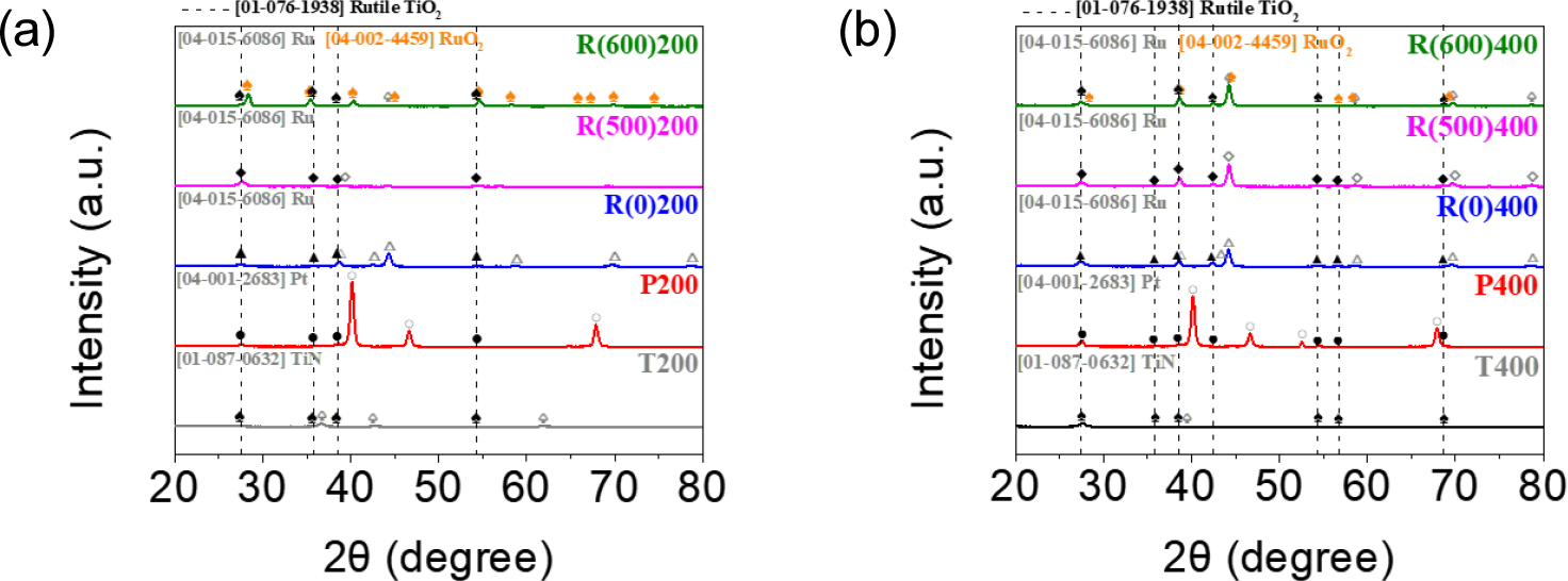
Table 1.
The average crystalline size of (110) and (211) plane in all samples.
Fig. 6 shows the surface morphology of each sample from AFM analysis. Table 2 shows the root-mean-square (RMS) roughness. Ru(600) samples have rougher surface morphologies compared to other samples. The pre-heating temperature of 600 °C for Ru is high, so Ru becomes oxidized and crystallized, which induces a much rougher TiO2 surface on it.

Table 2.
Roughness obtained by AFM analysis of T200, P200, R(0)200, R(500)200, R(600)200, T400, P400, R(0)400, R(500)400, and R(600)400.
| Sample | T200 | P200 | R(0)200 | R(500)200 | R(600)200 |
| RMS roughness [nm] | 2.219 | 1.950 | 1.489 | 1.905 | 7.097 |
| Sample | T400 | P400 | R(0)400 | R(500)400 | R(600)400 |
| RMS roughness [nm] | 1.501 | 2.148 | 2.078 | 1.341 | 9.052 |
Through I-V and C-V measurements, we evaluated the electrical characteristics of the devices. Fig. 7 shows the current density (J) - voltage (V) plot that illustrates the leakage current density occurring within the typical operating voltage range of DRAM. Fig. 7(a) shows the J-V plot of 200-cycle deposited samples, and Fig. 7(b) shows those of 400-cycle deposited samples. In Fig. 7(a), compared to the sample using TiN, all other samples show a reduction of leakage current density. The current density in R(600)200 was significantly decreased. When Ru was pre-heated at 600 °C, the temperature condition was appropriate to form RuO2, so the formation and crystallization of RuO2 were confirmed in XRD analysis. Therefore, the structural compatibility between rutile TiO2 and RuO2 causes reducing lattice mismatch, leading to reduce the leakage current density.12) In addition, larger grain size with (110) preferred orientation may contribute the reduction of leakage current in R(600)200. In Fig. 7(b), in the case of 400-cycle deposited samples, leakage current density is overall lower than 200-cycle deposited samples. In 400-cycle deposited samples, the leakage current density of R(600)400 is larger than T400. We consider that rougher surface roughness may induce the electrical field concentration at a local spot, which could result in a larger leakage current.25,26) Overall, the effect of leakage current reduction due to the substrate optimization was more pronounced in 200-cycle deposited samples.

Fig. 8(a, b) show the C-V characteristics of 200-cycle and 400-cycle deposited samples, respectively. In the C-V characteristics, the effect of substrate was apparent at 200-cycle deposited samples. In both 200 and 400 cycles, samples using Pt and Ru substrates have greater capacitance compared to the device with TiN. R(600)200 and R(600)400 show higher capacitance than other samples. It can be attributed that rutile (110) TiO2 with a large dielectric constant could be epitaxially grown along with RuO2, affecting the capacitance increment. The dielectric constants obtained from the measured capacitance values are presented in Table 3. In both 200 and 400-cycle deposited devices, the dielectric constants of all other samples are increased compared to those of T200 and T400. Especially, R(600)200 and R(600)400 show higher-k characteristics due to the preferential growth of rutile (110) TiO2. Several reports described that TiO2 on RuO2 can have a high dielectric constant of over 155, and we observed that the dielectric constant of R(600)200 samples was notably high.27) Note that the thickness was monitored by using Si substrates that were co-deposited during ALD deposition process, which may not provide precise thickness measurement depending on the substrate types. Particularly, in pre-heat treatment at 600 °C, surface roughness was significantly increased, leading to a larger thickness difference than other samples. In addition, there is a possibility that the formation of a TiO2-RuO2 interfacial layer could introduce errors in the thickness estimation. Although there is an inaccuracy in the thickness of TiO2 thin film, the formation of RuO2 and (111) rutile TiO2 could result in the increment of dielectric constant. Additionally, Lee et al.,28) reported that post-deposition treatment of the film by O2 plasma reduces oxygen vacancies and defects, resulting in improved quality of the TiO2-Si interface. The possibility of a decrease in oxygen vacancies through PEALD process could be attributed to this high dielectric constant. To prove the high dielectric constant in TiO2 on pre-heated Ru substrate, further deliberate study is necessary.
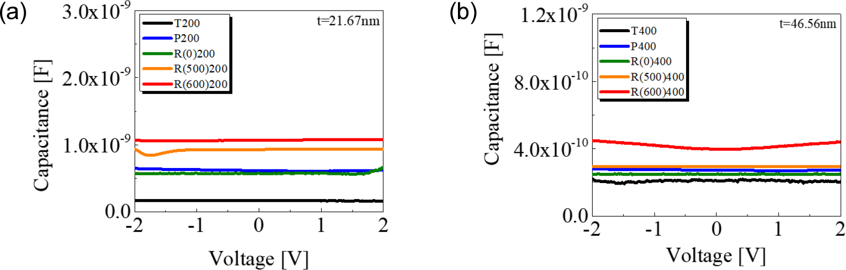
Table 3.
Summary of dielectric constant.
| Sample | T200 | P200 | R(0)200 | R(500)200 | R(600)200 |
| Dielectric constant | 23 | 85.2 | 79 | 126 | 147 |
| sample | T400 | P400 | R(0)400 | R(500)400 | R(600)400 |
| Dielectric constant | 62.43 | 80.43 | 73.35 | 86.51 | 119.30 |
Fig. 9 shows the relation between EOT and leakage current density at an applied voltage of 1 V. According to the 2023 IRDS roadmap, there is a demand for the development of integrated high-k dielectrics with ultra-low nanometer-scale EOT of less than 0.5 nm with low leakage current.29) According to the literature, the leakage current increases rapidly up to ~10-3 A/cm2 level when the EOT is less than 0.5 nm.30) We confirmed that the devices of TiO2 on pre-heated Ru showed the leakage current decreased to ~10-5 A/cm2 in the corresponding EOT of about 0.5 nm.

4. Conclusion
This study investigated the leakage current and capacitance characteristics of TiO2 thin film according to the use of PEALD with hollow cathode plasma source and various bottom electrode materials. For TiO2 thin films, the leakage current was substantial, and the interfacial properties with the poly-Si bottom electrode were unfavorable, limiting its application as the high-k dielectrics. To address this limitation, we employed PEALD to enhance the quality of the thin films and utilized transition metal nitrides and noble metals as the substrate materials, thereby mitigating the limitations of TiO2. We directly grew the rutile TiO2 on Ru by forming RuO2 on Ru oxidized at 600 °C. The analysis of electrical properties showed that the capacitance of 200- and 400-cycle deposited TiO2 on pre-heated Ru substrate increased by up to ~6 and 1.9 times higher compared to TiN control group. Moreover, the leakage current was decreased compared to that of the control group. By adjusting the phase and thickness of TiO2 and pre-heating conditions, we found the significant improvements in increasing capacitance at the 0.5 nm level of EOT with reduced leakage current. This can be applicable to the fabrication of capacitors in DRAM technology.
