

1. Introduction
2. Experimental Procedure
2.1. Device preparation
2.2. Resistive switching test
3. Results and Discussion
3.1. Physical and chemical characteristics
3.2. Resistive switching characteristics
3.3. Resistive switching mechanism
4. Conclusion
1. Introduction
The advancement of technologies such as big data and artificial intelligence (A.I) necessitates faster digital information processing compared to previous times.1) However, scaling down existing silicon-based semiconductor devices has limitations in achieving the required high-speed processing capability. Therefore, much research attention has been focused on next-generation memory devices.2) Among these devices, resistive random access memory (RRAM) has been extensively studied owing to its simple structure, fast operation speed, low power consumption, and excellent scalability of MIM (metal-insulator-metal).3,4,5,6,7) The functionality of RRAM relies on the resistive state change of the insulator. The conduction filament is formed through the SET process, where the insulator transitions from a high resistance state (HRS) to a low resistance state (LRS). The filament is ruptured through a RESET operation, which involves a change from LRS to HRS.
Resistance change properties have been observed in binary transition metal oxides such as TiO2, NiO, and ZnO,8,9,10) as well as in complex oxides like PrCaMnO (PCMO) and BaxSr1-xTiO3.11,12) Among materials with such characteristics, TiO2 stands out as a binary transition metal oxide due to its high density, simple structure, and fast switching properties.13) Therefore, TiO2 has been widely investigated as a resistive switching (RS) layer in RRAM devices.14,15) The fabrication of TiO2 thin films can be achieved through vacuum-based or solution-based deposition methods. Vacuum-based methods such as sputter, atomic layer deposition (ALD), and chemical vapor deposition (CVD) have been primarily utilized because of their excellent thickness control and uniform film formation.16) However, these processes have limitations in terms of cost and complexity.17) On the other hand, solution-based methods, such as spin coating and hydrothermal methods, offer low-cost, simple processes.2,18) Also, this process has the potential for fabrication of transparent thin films. Among these processes, spin coating has been extensively researched as a method for manufacturing RRAM devices due to its ability to produce thin films and ease of process control.19) To utilize the advantageous spin coating method, it is necessary to fabricate TiO2 as a solution-based material. Therefore, in a previous study, we synthesized TiO2 using the peroxo titanium complex (PTC)-ion method, which is eco-friendly and differs from the conventional TiO2 fabrication methods.20,21,22) Moreover, we successfully fabricated a TiN/TiO2/FTO structure RRAM device using PTC-ion solution and demonstrated successful resistance change properties.23) The insulator layer of the RRAM device was fabricated using a PTC-ion solution derived from eco-friendly materials, specifically TiO2. Unlike other solution-based TiO2 fabrication methods that utilize organo-metal or metal precursors, our PTC-ion synthesis method is safe for human and eco-friendly. However, while a ~45 nm thin film was successfully produced via spin coating, the resulting film’s uniformity was inferior to that obtained through vacuum deposition processes. Typically, uniformity and thinness are crucial for achieving low power consumption. Moreover, non-uniform films can lead to the formation of random filaments. Previous research optimized the spin coating process to produce a uniform film, but the issue of random filament formation still persists.
In order to regulate the formation of random filaments in RRAM devices, various studies have been conducted, such as the use of multi-layers or thin metal layers.24,25,26,27) Nevertheless, the presence of dipoles caused by heterojunctions in multi-layer structures can impede carrier movement, resulting in an increase in the forming voltage.28) Therefore, changes in device characteristics due to the introduction of precursor materials into TiO2 thin films have been reported.29,30) Moreover, since the process is solution-based, the precursor material can be introduced into the TiO2 thin film by simply adding it to the PTC solution. The insertion of metal ions is expected to influence the performance of RRAM devices by affecting filament formation. Various materials, such as Al and Ag, which are used as top electrodes in conductive-bridge random access memory (CBRAM) devices, are potential metal precursors. Among these, Ag can be promising candidate for the insertion of metal precursor. Due to Ag’s high mobility characteristics, it is widely used as an upper electrode in RRAM devices and has recently gained attention in the field of neuromorphic computing.31,32) However, as with excessive ion doping, excessive insertion of precursors can lead to deteriorated cycle characteristics, decreased resistance change, and reduced structural stability. Hence, identifying the optimal ratio is crucial.
In general, RRAM devices using TiO2 as an insulator layer exhibit behavior characteristic of oxygen vacancy resistive access memory (OxRAM), which involves conduction through the formation and rupture of filaments containing oxygen vacancies (Vo).33) On the other hand, CBRAM relies on a mechanism that involves the formation and rupture of conductive filaments through cations such as Ag or Cu that drift from metal electrodes.34) In the case of an RRAM device fabricated by inserting a metal precursor into the TiO2 layer, it is expected that a conduction mechanism involving both metallic ions and oxygen vacancies will arise, which is distinct from the general case. Since most insulator layers are fabricated by vacuum deposition, research on directly inserting metal precursors into the insulator layer has not been conducted much yet. Thus, it is crucial to comprehend the fabrication mechanism to effectively apply RRAM devices which inserted metal precursor.
In this study, we aimed to fabricate a TiN/Ag embedded TiO2/FTO RRAM device through a simple process of embedding Ag nanoparticles in a PTC solution. By optimizing the composition and processing temperature, we successfully confirmed the change in resistance switching characteristics. To investigate the effect of the Ag concentration on resistance change characteristics, we fabricated devices with AgNO3 concentrations of 0.3, 0.5, and 0.7 at%. We then analyzed the current-voltage (I-V) characteristics of the Ag embedded RRAMs and identified the appropriate concentration of AgNO3 precursor. Furthermore, by elucidating the new conduction mechanism, we were able to reduce the operating voltage through the conductive properties of Ag particles. Ultimately, we developed a reliable, eco-friendly, and low-temperature solution process based on PTC-ion.
2. Experimental Procedure
2.1. Device preparation
The PTC-sol was prepared using a jacketed beaker in the same manner as in our previous study while maintaining the reaction temperature below 50 °C, titanium hydride (IV) (TiH2, 99 %, Sigma-Aldrich) was added to a mixed solution of hydrogen peroxide (H2O2, 30 %, DAEJUNG) and ammonium hydroxide (NH₄OH, 25~30 %, DAEJUNG), after that followed by stirring for 1 h to stabilize the solution.23) An Ag-PTC-ion solution containing silver nitrate (AgNO3, 99 %, Sigma-Aldrich) ions of 0.3 at%, 0.5 at%, and 0.7 at% compared to Ti was prepared. The prepared PTC ion solution at room temperature was heated at 80 °C for 10 min and then cooled to a temperature of 15 °C or less again. Finally, it was completely dissolved to prepare a transparent Ag-PTC-ion solution. Fluorine doped tin oxide (FTO) glass surface to be used as an electrode was cleaned in order to prepare a uniform TiO2 thin film. 0.25 mL of the prepared Ag-PTC solution was dripped onto FTO glass through spin coating for 3,000 rpm, 30 s, 3 cycles, and then heat-treated at 100 °C to prepare a TiO2 thin film. Afterward, a titanium nitride (TiN) electrode having a diameter of 0.2 mm and a height of 100 nm was deposited by RF magnetron sputtering through a circular shadow mask.
2.2. Resistive switching test
The I-V curve measurements were conducted in DC voltage sweep mode using a Keithley 4200A-SCS semiconductor parameter analyzer. For the TiN/TiO2/FTO devices, DC bias voltages were applied incrementally at 0.05 V/step across a range of 0 ± 8 V. In instances where the FTO bottom electrode was grounded in the TiN/Ag embedded TiO2/FTO device, the DC bias was applied to the TiN top electrode at a step of 0.05 V within a sweep range of 0 ± 5 V, and a compliance current (C.C) of 0.1 A was implemented. The retention characteristics were verified through retention time measurements, while cycle durability was assessed by analyzing cycle characteristics. Furthermore, the I-V curves were subjected to linear fitting analysis during both positive and negative voltage sweeps to evaluate the device’s performance relative to the Ag content.
3. Results and Discussion
3.1. Physical and chemical characteristics
As shown in Fig. 1, it can be confirmed that a TiO2 thin film is deposited on the pristine FTO glass after 3 cycles of spin coating. As is well known, the thickness and uniformity of the RS layer affect the operating voltage characteristics of the device. So, a thin and uniform film is important for low voltage characteristics. As a result of further enlargement through TEM, it was confirmed that a dense TiO2 layer was deposited in the range of 50 to 100 nm. In general, PTC-ion solutions have low viscosity and high shrinkage, so it is difficult to prepare a uniform thin film. Through the process used in our previous study, a sufficiently uniform thin film was produced compared to other vacuum deposition processes.23) To determine the optimal RRAM device, X-ray photoelectron spectroscopy (XPS) analysis was performed to obtain information on the elements and chemical states of the samples. Fig. 2 displays the high-resolution XPS peaks of Ti (2p), O (1s), and Ag (3d) for the (a) pristine TiO2, (b) 0.3 at% embedded TiO2 and (c) 0.5 at% embedded TiO2 RRAM devices. The Ti (2p3/2) peaks were respectively 458.17 eV and 456.86 eV in (a). Also, 0.3 at% Ag embedded TiO2 RRAM device in (b) show characteristic peaks at 458.18 eV and 456.83 eV, which correspond to Ti4+ and Ti3+, respectively.23) Similarly, according to (c), the 0.5 at% Ag embedded TiO2 RRAM device appear at 458.18 eV and 456.98 eV. It was confirmed that TiO2 was successfully formed in all samples. Compared to the (a), intensity of Ti was decreased by the addition of Ag. It goes with the formation of Ti3+ also decreased. Ti3+ is generated by the formation of oxygen vacancies, and it acts as a defect.35) However, it shows that the ratio of Ti3+ in (c) is increased compared to (b). This seems to affect oxygen vacancies by increasing the formation of Ag-O bonds due to excessive Ag intercalation. The presence of many oxygen vacancies can lead to a decrease in operating voltage. However, as SET/RESET switching is repeated, cycle stability may be adversely affected due to the reduction of oxygen ions. Additionally, the defect site inside can act as an electron trap site and can have an electrical effect on the device. The O (1s) peak exhibits characteristic peaks at 529.67 eV, 531.33 eV, which correspond to Ti-O, -OH respectively. In (b), the binding energy of O (1s) are 529.64 eV, 530.73 eV, 532.07 eV, and 532.4 eV, which correspond to Ti-O, Ag-O, -OH, and O2.36,37) Similarly, respectively bondings were characterized at 529.7 eV, 530.79 eV, 532.13 eV, and 532.52 eV in (c). In (b) and (c), the presence of Ag-O peaks was confirmed following the insertion of Ag. A notable change was observed in the -OH peak. Unlike the RRAM devices in the (a), both samples showed a significant increase in the area of the -OH peak, which seems to have resulted from the interaction between Ag and TiO2. The amount of Ag-O bonding slightly increased with the addition of Ag. Unlike (a), Ag (3d5/2) spectra of (b) and (c) were characterized at 367.67 eV and 367.62 eV, respectively. Each sample is divided into 367.5 eV, 368.01 eV, and 367.53 eV, 368.13 eV, which correspond to Ag+ and Ag0, respectively.38) An increase in intensity was confirmed with the addition of Ag. Additionally, Ag exists more as Ag+ than Ag0, which corresponds to the Ag-O peak in the O (1s) peak. The binding energy of bulk Ag (3d5/2) was assigned at 368.3 eV, and both samples were shifted to the lower position.39) These results are likely due to the strong interaction of electrons moving from TiO2 to metallic Ag.37)


3.2. Resistive switching characteristics
Based on the results of previous studies, the basic characteristics of the Ag embedded TiO2 RRAM devices were investigated by applying a voltage sweep range of 0 ± 8 V with a consistent C.C value of 0.1 A.23)Fig. 3 illustrates the I-V curve under the condition of 0.3 at% Ag embedded TiO2 RRAM. Initially, during the positive voltage sweep, the current level gradually increased, leading to a SET operation at +3.7 V. This was followed by maintaining the LRS during the reverse voltage sweep, where the RESET operation occurred at -3.7 V. The investigated I-V curve results showed a variance from those of conventional OxRRAM. Firstly, compared to OxRRAM, the initial resistance value was increased by four orders of magnitude, resulting in a low initial resistance value of 10-6. Furthermore, it was observed that the SET/RESET voltage significantly decreased to -3.7 V/3.7 V according to the voltage sweep range. This indicates that the addition of Ag altered the resistance characteristics of the TiO2 layer, and the material forming filaments shifted to metallic filaments, exhibiting characteristics of CBRAM. As the SET/RESET voltage range decreased, sweeping at unnecessarily high voltage ranges could stress the device. Therefore, the voltage sweep range was reduced to ±5 V, and simultaneously, the C.C was decreased by one order of magnitude to apply a current of 10 mA. Under these modified conditions, Fig. 3 characterizes the I-V curves of Ag embedded TiO2 RRAM with varying Ag content.

Electrical analysis was conducted on TiN/Ag-embedded TiO2/FTO RRAM devices with varying Ag content (0.3 at%, 0.5 at%, and 0.7 at%), to investigate the effect of Ag concentration on resistance switching characteristics. Fig. 4(a) illustrates the I-V curve of the RRAM device with 0.3 at% Ag, indicating typical nonvolatile bipolar RS behavior. During the negative voltage sweep, the current gradually increases, and a SET process (transition from HRS to LRS) occurs due to a rapid rise in current level at Vset: ~-3 V. On the other hand, during the positive voltage sweep, LRS is maintained, and a RESET process (transition from LRS to HRS) occurs through a sudden drop in current at Vreset: ~3 V. The TiN/0.3 at% Ag-embedded TiO2/FTO RRAM device showed successful RS characteristics, reaching the initial resistance value of 10-8. Similarly, the RRAM device embedded with 0.5 at% Ag also showed RS behavior, as shown in Fig. 4(b), with a gradual rise in current during the negative voltage sweep, and a SET process at Vset: ~-2 V. During the positive voltage sweep, LRS is maintained, and a RESET process occurs at Vreset: ~2.4 V. Therefore, the TiN/0.5 at% Ag-embedded TiO2/FTO RRAM device also showed successful RS characteristics, reaching an initial resistance value of 10-8. However, when the Ag content was 0.7 at%, complete ohmic conduction characteristics were observed, with the absence of SET and RESET processes. The initial resistance of the TiN/0.7 at% Ag embedded TiO2/FTO RRAM device was greatly reduced, with an initial resistance value of 10-6, unlike the 0.3 at% and 0.5 at% embedded RRAM devices. Hence, at high Ag concentrations, it appears that the resistance change layer does not function as an insulator. While the RRAM devices with 0.3 at% and 0.5 at% Ag were successfully behaved as RRAM devices, the 0.7 at% embedded RRAM device did not. As the content of Ag increased from 0.3 at% to 0.5 at%, the Vset and Vreset of the RRAM device decreased, likely due to an increase in the proportion of Ag ions forming filaments. Furthermore, the Vset and Vreset of the RRAM device with 0.3 at% and 0.5 at% embedded Ag were significantly reduced compared to the TiN/TiO2/FTO RRAM device fabricated in a previous study, with a reduction of about 4 V or more each.23) Despite having the same thickness, the values of Vset and Vreset decreased by more than half depending on the Ag content. In general, the resistance change characteristic in binary oxide-based devices is caused by the formation and rupture of filaments by oxygen ions.40) However, in the case of TiO2 layers containing Ag, a change in the conduction mechanism is expected to occur due to the formation of a conduction bridge by the movement of Ag ions.

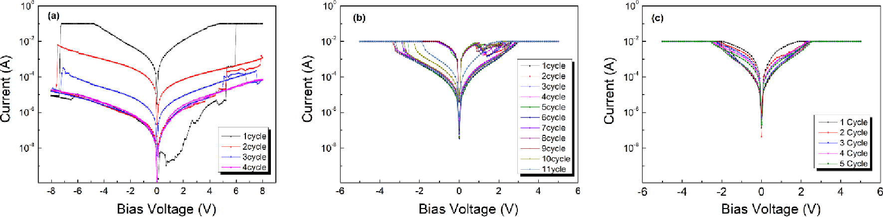
Fig. 5 illustrates the cycle characteristics of the RRAM device according to content of Ag. As Ag is inserted, cycle performance is improved. In Fig. 5(a), resistance change characteristics no longer appear after 4 cycles. This is because O2- ions generated by cycle repetition in the RS layer made of pristine TiO2 combine with each other and lose as O2. However, in the case of Fig. 5(b), the number of escaped O2- is reduced due to the presence of Ag, resulting in improved stability. And it shows that the resistance change characteristics were consistently maintained up to 10 cycles. The insertion of Ag ostensibly enhances cycle performance. On the other hand, the RRAM device containing 0.5 at% Ag embedded TiO2 in Fig. 5(c) could not maintain the resistance change characteristics as the cycle number increased, and the device showed ohmic conduction behavior after only 5 cycles. While low Ag content improves device stability by reducing the loss of O2- ions, leading to enhanced cycle performance, a higher Ag content (0.5 at%) introduces challenges. The RRAM device with 0.5 at% Ag exhibits ohmic conduction behavior after a limited number of cycles due to the incomplete oxidation of Ag filaments. Similar to the behavior of a typical CBRAM device, when an opposite voltage is applied to the device, the Ag filament is oxidized to Ag+.41) The excessive Ag leads to a build-up of unoxidized Ag atoms, adversely affecting the device’s resistive switching characteristics.42) Therefore, the application of the RRAM device containing 0.5 at% Ag as a reliable memory device is limited. In addition to cycle performance, the retention time is an essential factor in evaluating the performance of a memory device.43)
The retention characteristics of the pristine TiO2 and 0.3 at% Ag-embedded TiO2 RRAM device are presented in Fig. 6. Both devices were shown a stable current level in both HRS and LRS for a period of 3,600 s, which is consistent with the retention behavior observed in typical RRAM devices.42) Additionally, the ON/OFF ratio for the pristine device (a) was measured at 104, and for (b), it was found to be greater than 103, aligning with the values derived from the I-V curve. For a non-volatile memory to be useful in practical applications, the ON/OFF ratio value should typically be at least 10 times higher than the reported value.44,45,46) Therefore, the observed ON/OFF ratio value of 3 orders of magnitude or greater confirms the suitability of the implemented device for use as a non-volatile memory. In addition, considering the above cycle stability, it was confirmed that Ag was inserted at 0.3 at% as optimal.
3.3. Resistive switching mechanism
Previous measurements of the current-voltage characteristics have indicated that the TiN/Ag embedded TiO2/FTO device operates through filament formation and migration of Ag ions as well as filament formation by oxygen vacancy. However, to fully comprehend the dominant mechanism of the TiN/Ag-embedded TiO2/FTO device for its practical application, it is necessary to confirm the conduction mechanism. Therefore, we analyzed the conduction mechanism of 0.3 and 0.5 at% Ag samples, where resistance change characteristics were observed. Fig. 6 show the I-V curve and double- logarithmic plot of TiN/Ag-embedded TiO2/FTO devices with 0.3 at% and 0.5 at% Ag content. The conduction mechanism was confirmed by performing linear fitting of I-V curves during positive and negative voltage sweeps. As shown in Fig.7(a), for the 0.3 at% Ag sample, the slope at high voltage during the negative bias sweep was found to be 2 or more, and a sudden increase in current was observed, confirming the dominance of the SCLC mechanism. The linear fitting of the 0.3 at% Ag sample also showed a slope of 1.4 during the negative bias sweep at high voltage. Typically, a slope close to 1 indicates either no current flow due to high resistance or ohmic conduction resulting from internal thermal carriers. However, since the slope was found to be higher than 1, the conduction mechanism can be attributed to Schottky emission (log(I)∝V0.5) during the low voltage range of 0~1 V in the HRS state. The direction and shape of filament formation by Ag ions are determined by the mobility of cations and the reduction rate of ions in the dielectric.37) In the case of the TiN/Ag embedded TiO2/FTO device, Ag ions move to the TiN electrode at a negative bias to form a tip, as the mobility of Ag ions is higher than the reduction rate. Therefore, the gap between the upper and lower electrodes is reduced due to the formed tip, resulting in a reduction in resistance and facilitating filament formation, leading to conduction by Schottky emission.

Subsequently, at voltages between 2 to 3.1 V, the 0.3 at% Ag sample exhibits a slope of 3.1, accompanied by a sharp increase in current, which is dominated by the trap-limited space charge limited current (SCLC) conduction mechanism (I∝V2). At this point, the injected carriers conduct a more significant role in determining the conduction characteristics due to an increase in carrier injection as compared to thermally generated carriers in the thin film. This phenomenon arises from the formation of a conductive path through the filament, which has been previously reported in Ti/Al2O3/AgNPs/Al2O3/p-Si structures, where Ag atoms and oxygen vacancies form filaments together.41) The conductivity is substantially enhanced during this period, leading to the SET process. Oxygen vacancies () migrate towards TiN in response to the negative voltage applied to the top electrode, forming filaments that follow the previously formed Ag ion tips. Additionally, Ag particles act as seeds in the conductive filament, reducing the randomness of filament formation and decreasing the conductivity path of the filament.47) In the following -1 V to 0 V sweep range, the slope of the 0.3 at% Ag sample is 1.2, indicating ohmic contact (I∝V) conduction. Similarly, during the 0 V to 0.9 V sweep range, which corresponds to a positive bias, the slope is 0.96, confirming the ohmic contact (I∝V) characteristic.48) This indicates that the positive bias applied to the top electrode is insufficient to break the hybrid filament composed of Ag atoms and oxygen vacancies. After that, the RESET voltage is reached, and the slope up to ~2 V is 4.9, demonstrating the trap-limited SCLC conduction mechanism. The slope during the 2 V to 0 V range is 1.7, following the Schottky emission mechanism. In the case of the 0.5 at% Ag sample, the result of the linear fitting in Fig.7(b) shows that the slope at high voltage has a value of 2 or more during the sweep to negative bias, accompanied by a sudden increase in current, confirming the dominance of the SCLC mechanism. However, the linear fitting result of the RRAM device containing 0.5 at% Ag, as shown in Fig.7(b), exhibits a high slope. As the Ag content increases, the amount of Ag that forms the filament increases, exhibiting characteristics that are consistent with the ionic conduction model. This outcome indicates that, unlike the 0.3 at% embedded RRAM, Ag becomes the primary component constituting the filament. The slope of the ionic conduction model can be calculated as follows.49)
The current density J, applied voltage V, temperature T, and a constant d are the parameters involved in the calculation of the slope in Fig. 7(b). Specifically, the HRS in Fig. 7(b) exhibited a slope of 1.6, while the slope increased to 4.1 in the LRS after the SET voltage was applied. The LRS slope was maintained at 1.7. When the RESET voltage was applied, a high slope of 4.8 was observed, although no current jumping was detected. This behavior is typical of CBRAM, where the metallic ion forming the filament is reduced to the top electrode during RESET operation and disappears within the insulator. However, even after reduction, Ag ions remain inside the insulator in Ag-inserted devices. As demonstrated by the previous cycle characteristics, excessive Ag content inside the insulator reduces device resistance and degrades RRAM performance, such as the ON/OFF ratio. Therefore, these results indicate that the electrical behavior and conduction mechanism in the RRAM device are affected by the Ag content, and the optimal performance is achieved when 0.3 at% of Ag is incorporated.

Based on the results described above, we present a model of filament formation through the movement of Ag ions and oxygen vacancies, as illustrated in Fig. 8. In the pristine state, before any voltage is applied, Ag is present in the TiO2 layer in the form of Ag+ and Ag atoms.28) TiO2 generally exists in a non-stoichiometric form, TiO2-x, where x represents a non-stoichiometric amount.50,51) The presence of non-stoichiometric amounts is typically caused by gaps in titanium or oxygen vacancies, with the latter resulting from insufficient oxygen supply during the deposition of TiO2.52) As such, oxygen vacancies are already present in the TiO2 layer even before the application of any voltage. When a negative voltage is applied, Ag ions in the TiO2 layer move towards the TiN electrode, while Ag atoms are oxidized and also move towards the TiN electrode in the form of Ag+. The moved Ag ions are reduced to form Ag atoms, which then form tips.53,54) Meanwhile, O2- ions move towards the positively biased lower electrode, where they are converted into O2 molecules. As a result, numerous oxygen vacancies are formed at the lower electrode interface.55) As the negative bias becomes stronger, the formation of oxygen vacancies increases from the FTO direction (positive bias), leading to the formation of filaments. At the same time, Ag filaments are formed from the TiN direction, which is the opposite direction. The two filaments eventually connect, leading to the SET process. When a positive bias is applied to the upper electrode, the joule heat generated by the thermal effect causes the oxygen vacancy and Ag atom filaments to be cut, leading to the RESET process. However, due to the lower activation energy of oxygen vacancies, the breakdown of the filament occurs faster than that of Ag atom filaments.47) Additionally, most of the positive bias applied to the upper part of the two positive charge types, oxygen vacancies, is pushed to the opposite side, resulting in the rupture of the filament. In contrast, in the case of Ag atom filaments, an electrochemical process involving overvoltage is required for Ag, which is an atom, to return to ions. As a result, the rupture of the filament mainly occurs in oxygen vacancy filaments, while Ag filaments remain almost unchanged.

4. Conclusion
In this study, we confirmed the electrical properties of TiN/Ag-embedded TiO2/FTO RRAM devices fabricated using a eco-friendly PTC-ion solution-based process with AgNO3 precursor added in varying concentrations. Comparing the I-V curves of devices with varying AgNO3 precursor concentrations reveals that RRAM devices with 0.3 at% and 0.5 at% Ag content display resistive switching (RS) characteristics, whereas devices with 0.7 at% Ag do not. The device with 0.5 at% Ag shows lower switching voltages than the one with 0.3 at% but has a reduced difference in current levels between high and low resistance states and lower initial resistance. Additionally, the 0.3 at% Ag device retains its switching characteristics for over 10 cycles, outperforming the 0.5 at% Ag device, which fails after 5 cycles.
Therefore, it was confrimed that the addition of Ag to the TiN/TiO2/FTO RRAM device can effectively prevent random filament formation and produce uniform RRAM devices with desirable electrical characteristics. By analyzing the I-V curves of different Ag content samples, it was found that 0.5 at% Ag content provided only suitable I-V characteristics, while 0.3 at% Ag content showed suitable I-V curve, ON/OFF ratio and long retention times. The conduction mechanism of the each RRAM device was also analyzed, showing that the electrical behavior and conduction mechanism varied with the Ag content. Through optimization of the Ag content, this study successfully overcame the limitations of the TiN/TiO2/FTO RRAM device, reducing SET/RESET voltage and C.C current, and improving cycle characteristics. In conclusion, our research presents a thorough analysis of cycle performance and retention characteristics under varying Ag contents, providing a comprehensive understanding of the necessary trade-offs and optimization strategies for developing high-density, low-power RRAM applications. This paves the way for its application in the advanced fabrication processes of RRAM devices, signifying a substantial step forward in the field.
