1. Introduction
2. Experimental Procedure
3. Results and Discussion
3.1. Results
3.2. Discussion
4. Conclusion
1. Introduction
Thermoelectric conversion (TEC) materials are expected to convert the thermal energy into electric energy without chemical reaction. It has attracted attention in recent years as an eco-friendly power generation system. The efficiency of TEC materials is verified by the material-specific dimensionless figure of merit ZT, which is defined as ZT = S2Tρ-1κ-1, where S is the Seebeck coefficient, T is the absolute temperature, ρ is the electrical resistivity, and κ is the thermal conductivity.1,2) Goldsmid et al.3,4) reported Z ~ 1.8 ‧ 10-3 K-1 and ~ 2.2 ‧ 10-3 K-1 for p-type and n-type Bi2Te3 in 1954. Assuming application at room temperature (R.T.), the p-type and n-type Bi2Te3 has been established as TEC materials with ZT ~ 0.54 and 0.66.4) Their achievement was stimulating further research in an energy harvesting technology. Subsequent studies enhance ZT values; e.g. p-type Bi0.5Sb1.5Te3 and n-type Bi2Te2.7Se0.3.5,6,7) Novel TEC materials, which exhibit the higher performance than those of Bi2Te3-based compounds at temperatures range of 300~600 K, will be a critical discovery in energy harvesting technologies.8,9)
Since the early 2000s, mixed anion layered compounds (MALCs) have been potential candidates for various electrical and electronic applications. A representative MALC LaCuChO (Ch = S, Se), which belongs to the tetragonal P4/nmm space group, exhibits a layered structure, with alternating layers of carrier blocking La2O2 and carrier conducting Cu2(S, Se)2 along to the c axis.10,11) LaCuChO compounds have been reported as a promising transparent semiconductor with p-type polarity and a degenerated semiconductor phase in the form of epitaxial thin films.12,13,14,15) The actual origin of p-type conduction was reported to be due to conducting holes generated by Cu off-stoichiometry and/or crystallographic defect of Cu in LaCuChO.16,17) On the other hand, BiCuSeO, which exhibits a layered structure as well as LaCuChO, was reported as a promising TEC material by Zhao et al.18) Research has been actively continued on carrier-doped BiCuSeO. ZT of BiCuSeO-based compounds reached a higher ZT > ~119,20) at T = 850 K. Wang et al.21) reports a theoretical high ZT for LaCuChO compounds using a rigid band model without assumed dopant. Their report estimates that LaCuChO-based compounds probably work as high-performance TEC materials as well as BiCuSeO-based compounds. However, the theory in which inevitable crystallographic defects were not provided, remains optimistic, and experimental results have yet to validate these predictions.
The transport phenomena in LaCuChO are complex. Ishikawa et al.22) report the ρ of the polycrystalline LaCuSO decreases with increasing T like a semiconductor from 300 K to 573 K, while the S increases with increasing T like a metal from 595 K to 670 K. Yasukawa et al.23) reports that the ρ-T curve is like a semiconductor for a polycrystalline LaCuSeO from 373 K to 673 K, while the S increases with increasing T like a metal from 373 K to 673 K. These results demonstrated that semiconducting behaviors were observed for ρ-T curves, while metallic behaviors were observed for S-T curves in these polycrystalline LaCuChO (Ch = S, Se).
According to Jonker24)’s S vs. Log10 (σ/σmin.) plot (Jonker plot) for a p-type semiconductor, the Jonker plot exhibits a negative straight line in carrier-doped extrinsic region. As shown in the Fig. 1, “undoped LaCuSeO HP, P//, Kato et al.25)”, “undoped LaCuSeO HP, P⊥, Kato et al.25)”, and present results are almost in accord to the Jonker plot that might be indicated by the slashed line, whereas several plots exhibit variation from the Jonker plot. “LaCu1-δSO, δ = 0.01, Goto et al.16)”, in which a band-renormalization might be demonstrated stimulated by the Fermi energy (EF) lower than valence band maximum (EV), is not on the Jonker plot. “undoped LaCuSeO SPS, Yasukawa et al.23)”, in which some chemical and morphological inhomogeneities might be included due to SPS process,26) exhibit positive gradient that is opposite to our present results.
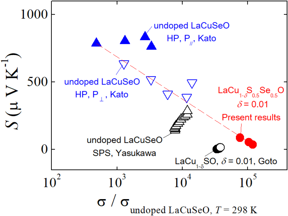
Fig. 1.
Seebeck coefficient (S) of LaCu1-δChO (Ch = S, Se) versus electrical conductivity (σ) divided by a conductivity measured at 298 K for a polycrystalline undoped LaCuSeO prepared under ambient pressure (AP) (σundoped LaCuSeO, T = 298 K). σundoped LaCuSeO, T = 298 K is reproduced from datum in Kato et al.25) “undoped LaCuSeO HP, P//, Kato” and “undoped LaCuSeO HP, P⊥, Kato”, which were measured for hot pressed polycrystalline samples, are also reproduced from data Kato et al.25) “undoped LaCuSeO SPS, Yasukawa”, which were measured for a polycrystalline sample obtained via Spark plasma sintering (SPS), is read from Yasukawa et al.23) “LaCu1-δSO, δ = 0.01, Goto”, which is measured for a polycrystalline sample prepared under AP, are reproduced from data Goto et al.16) “LaCu1-δS0.5Se0.5O δ = 0.01” is calculated from present results. The slashed line is a guide for eyes.
The mechanism of the transport properties had been controversial for LaCuChO (Ch = S, Se). The composition of the sample plays a crucial role in influencing the transport properties, leading to the coexistence of both semiconducting and metallic behavior. To clarify the transport mechanisms, further verification through X-ray diffraction (XRD) analysis is necessary. However, the absence of XRD data in previous reports complicates this verification. Therefore, this manuscript aims to provide a detailed characterization of the sample, including XRD data, to evaluate its transport properties, specifically the electrical resistivity, thermal conductivity, and Seebeck coefficient.
Detailed mechanism of the p-type conduction is explained based on several literatures in following paragraphs. Hiramatsu et al.15) reports a resistivity (ρ) of a few 10-2 Ωm in an undoped LaCuSeO epitaxial thin film at R.T. Based on density functional theory, a carrier generation mechanism is attributed to Cu cation defects in a crystallographic site for LaCuChO, whose mother compound is an insulator with a wide optical band gap. Such transport properties of the undoped LaCuSeO epitaxial thin film is a typical degenerate semiconductor,17) which are not anomalous conductors in practical electrical conducting compounds, i.e. transparent semiconductors.13) Goto et al.16) reports that ρ of polycrystalline LaCu1-δSO, in which δ ~1 at% of Cu defects is introduced into the polycrystalline LaCuSO, exhibits 2.6 ‧ 10-3 Ωm that is one million times lower value than that of an undoped LaCuSO.
Kato27) had attempted to synthesis high density carrier doped LaCuSeO by introducing Cu defects, while the electrical resistivity (ρ) of the obtained samples, exceeded 1 Ωm at R.T. Kato27) failed to obtain polycrystalline highly carrier doped LaCuSeO that had been reported for epitaxial thin film.15) The relatively high ρ ≥ 1 Ωm for the polycrystalline LaCuSeO samples with nominal Cu defects indicates that the polycrystalline LaCuSeO with nominal Cu defect is an insulator rather than the degenerate semiconducting phase.27) It is noted that resistivity ρ of the nominal Cu defected samples, which are prepared as nominal off-stoichiometric compositions,27) exhibits the far higher ρ than those of the undoped polycrystalline LaCuSeO samples prepared via hot-press synthesis.25) Kato27)’s report indicates that there are qualitative differences of carrier doping mechanism between polycrystalline bulks and epitaxial thin films in LaCuSeO.
In a contrary, Azuma et al.28) reports the ρ of a polycrystalline LaCuS0.5Se0.5O with δ ~1 at% of Cu defects (LaCu0.99S0.5Se0.5O) was about 6.8 ‧ 10-4 Ωm at R.T. The ρ is one million times lower than that of insulating undoped LaCuS0.5Se0.5O at R.T.28) Surprisingly, the ρ is lower than that of the epitaxial thin film, which is reported by Hiramatsu et al.15) with a carrier concentration of about 2 ‧ 1019 cm-3, a Hall mobility of about 4 cm2 V-1 s-1 and a ρ of about 1.0 ‧ 10-3 Ωm at R.T. In these LaCuS0.5Se0.5O samples, Cu defects indeed generate carriers in both of epitaxial thin films and polycrystalline bulks, although the detailed effects of Cu defects, grain boundaries, and orientation on transport phenomena and their physical mechanisms, which lead common understanding in transport properties, are still unknown.
Details of the δ dependence and sample preparation dependence had been discussed in previous reports28,29) with sample purity and transport properties. It is noted that the δ = 0.02 sample (LaCu0.98S0.5Se0.5O) exhibits the XRD pattern without second phases, however the ρ of the δ = 0.02 is larger than the δ = 0 electrical insulating sample. The larger ρ of the δ = 0.02 is probably due to possible (S, Se) vacancies, which are created to compensate the charge imbalance due to Cu vacancies. The δ = 0.02 is insulator indicating that the electrical conduction mechanism of LaCu1-δS0.5Se0.5O (δ > 0.02) is more complex and above our scope. In the present report, our results and discussion are limited on the LaCu1-δS0.5Se0.5O δ = 0, 0.01.
Slight amount of Cu deficient results a variety of ρ ranged from ~103 to ~10-3 Ωm for nominal LaCuS0.5Se0.5O samples. In a report by Azuma,29) seven nominal LaCu1-δS0.5Se0.5O (δ = 0) samples were prepared using same nominal precursor and several heat treatment temperatures at T = 1,000~1,080 °C. Three nominal δ = 0 samples exhibit insulating electrical properties with ρ ~1.0 ‧ 103 Ωm, while one nominal δ = 0 exhibits degenerate semiconductor phase with ρ = 1.1 ‧ 10-3 Ωm. Other three samples were too fragile to cut into a square column for 4-probe DC resistivity measurements. In present engineering, our group has not established a perfect production control on the synthesis of LaCu1-δS0.5Se0.5O, although we can evaluate slightly different lattice constants each other.28)
In this manuscript, the characterization of the polycrystalline LaCu1-δS0.5Se0.5O (δ = 0.01) is presented, and its thermal properties are revealed for the first time at T ≤ 673 K. The δ = 0.01 sample exhibits metallic ρ-T and metallic S-T curves as a typical degenerate semiconducting phase. Present results also suggest that understanding for the relations among ~1 at% crystallographic defect, thermal transport properties and these mechanism are still controversial.
2. Experimental Procedure
Polycrystalline LaCu0.99S0.5Se0.5O sample was prepared using nominal composition by solid-state reaction in a sealed silica tube.28) The powder was pelletized using cold pressing with P = 20 MPa under Ar atmosphere before the solid-state reaction in a sealed silica tube. Detailed procedures and characterizations were reported in Azuma et al.28) Purity of the obtained sample was examined by XRD using CuKα radiation (Rigaku Rint 2500, Japan).
Artificial crystallographic orientation of the polycrystalline sample was not applied in our synthesis procedures, although a certain degree of the crystallographic orientation might appear in the polycrystalline sample. In this report, the degree of the crystallographic orientation in the polycrystalline sample has not been investigated. Transport properties of the sample were measured along and vertical direction to the cold pressing.
Resistivity (ρ) of the sample was measured by DC four-probe technique at T = 300~673 K. Seebeck coefficient (S) and thermal conductivity (κ) of the sample were measured using the steady-state method at T = 473~673 K. In both the four-probe technique and the steady-state method, the temperature (T) was controlled by a commercially supplied program for an infrared lamp heating system (Advance Riko MILA-5000, Japan). Gold (Au) was coated as the electrode, and platinum wire (Nilaco PT-351105, Japan) was used as the conductor, which was bonded to the electrode with silver paste (Dupont 6838, USA). Detailed of our measurement are as follows.
In the steady-state method, the sample was cut into dimensions of approximately 2 × 2 × 7 mm3. A heater was affixed to the top surface of the molded sample, inducing a temperature gradient across it. The sample’s average temperature was determined using R-type thermocouples attached to both its top and bottom surfaces, while the MILA-5000 controlled the temperature to achieve the desired conditions. However, when attempting to apply a temperature difference to both ends of the sample at room temperature, it becomes challenging to maintain precise control over the device’s temperature.
The measurement of the Seebeck coefficient involved plotting the thermoelectric voltage generated between the high-temperature and low-temperature sides of the sample due to the induced temperature gradient by the heater. The intrinsic Seebeck coefficient of the sample was then derived by subtracting the known Seebeck coefficient of the conductor (Pt) from this value.
Thermal conductivity (κ) was determined using both the steady-state and laser flash methods. In the steady-state method, the slope of multiple plots of temperature gradient versus heat flux had been used to demonstrate Fourier’s law. Heat flux was primarily calculated as Joule-heat generated from the heater. However, it was partly influenced by heat conduction losses from the sample to the thermocouple and heat radiation losses from both the sample and thermocouple to the furnace wall.30) The steady-state method, owing to its resemblance to practical thermoelectric power generation, show a potential applicability of the sample in practical condition. The uncertainty in measured thermal conductivity values was evaluated to be approximately 10 % when compared to results from standard samples.2)
Thermal conductivity (κ) of the sample was also obtained using a product of thermal diffusivity, specific heat capacity, and density of the sample. The thermal diffusivity was measured by laser flash equipment (Ulvac TC7000, Japan), at 300 K, 353 K, 403 K, 463 K and 513 K. The thermal diffusivity was measured for the sample with a diameter of 10.2 mm and a thickness of 2.8 mm. Specific heat of the sample was measured using relaxation method. The density of the sample was measured using caliper and electronic balance.
3. Results and Discussion
3.1. Results
Fig. 2 shows the XRD pattern and picture of polycrystalline LaCu1-δS0.5Se0.5O (δ = 0.01) sample. Here, vertical bars (|) at the bottom represent diffractions from pure LaCuS0.5Se0.5O.11) The dominant phase of the sample was LaCu1-δS0.5Se0.5O (δ = 0.01), although there is a weak peak probably assigned to La2O2Se and/or La2(SeO3)3 exhibiting a 4.8 % relative peak intensity. The sample has a porosity of 45 vol%. Although the sample has a porosity of 45 vol%, it remains suitable for measurement and evaluation purposes. Even though it is porous, the sample is not fragile; it maintains a solid and rigid structure, allowing for accurate assessment of its properties. Table 1 shows lattice constants (a and c) and lattice volume (V) for LaCu1-δS0.5Se0.5O (δ = 0, 0.01, 0.02) samples. The lattice constant a was 0.4034 (1) nm and the value of c was 0.8656 (4) nm for the present sample. As shown in Table 1, the δ = 0.01 sample exhibits smaller lattice parameters compared to the undoped samples (δ = 0, pure, weakly doped).28) Decrease in the lattice volume indicates that the introduction of copper defects generating carriers contribute the decrease in lattice volume at δ = 0~0.01.
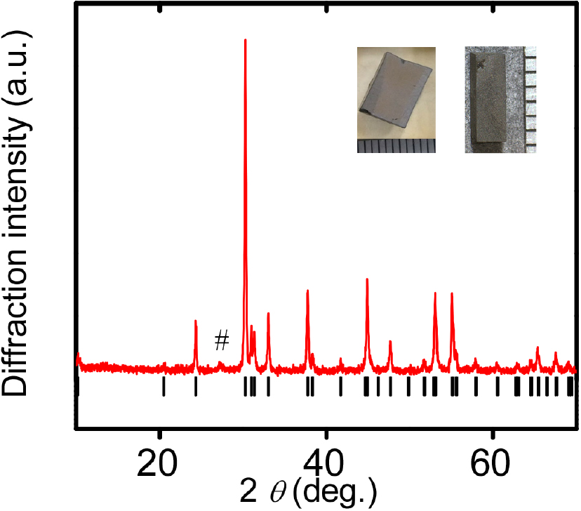
Fig. 2.
X-ray diffraction (XRD) pattern of polycrystalline LaCu1-δS0.5Se0.5O (δ = 0.01). The vertical bars at the bottom represent calculated positions of LaCuS0.5Se0.5O.11) The number sign (#) denotes Bragg diffractions due to La2O2Se and/or La2(SeO3)3. The photo on the left in the figure shows a synthesized sample. The photo on the right in the figure shows a sample molded for the steady-state method measurement.
Table 1.
Lattice parameters, and resistivity (ρ) of polycrystalline LaCu1-δS0.5Se0.5O (δ = 0.01, 0.02) and undoped LaCuS0.5Se0.5O samples (δ = 0, pure, weakly doped) with referenced results.11,28,31) Weakley doped and pure were prepared using nominal chemical composition LaCuS0.5Se0.5O. Characterization of the samples is reported in Azuma et al.28) The pure was too fragile to cut into a square column for 4-proved DC resistivity measurements.
| ρ (Ωm) | a (nm) | c (nm) | V (nm3) | |
| Ueda et al.11,31) undoped | ~50 | 0.4035 | 0.8661 | 0.1410 |
| Azuma et al.28)δ = 0 | 1.0 × 10³ | 0.4042 (10) | 0.8684 (28) | 0.1419 (10) |
| Pure | N/A | 0.4040 (4) | 0.8665 (7) | 0.1414 (3) |
| weakly doped | 1.1 × 10⁻³ | 0.4037 (6) | 0.8660 (12) | 0.1411 (5) |
| δ = 0.01 | 6.8 × 10⁻⁴ | 0.4034 (1) | 0.8656 (4) | 0.1408 (1) |
| δ = 0.02 | 1.9 × 10³ | 0.4032 (3) | 0.8648 (5) | 0.1406 (2) |
Fig. 3 shows the relationship between heat flux (q) and temperature gradient (ΔT/z) to determine the κ in steady-state method, where z is the distance between two R-type thermocouples attached to an upper and a lower point in the sample surface. The heat flux passing through the sample was determined by the electric current flowing through the heater. Furthermore, the temperature gradient was calculated by dividing the temperature difference (ΔT) between the upper and lower points by the distance (z) between the points. The κ was determined as the slope in q as a function of ΔT/z.
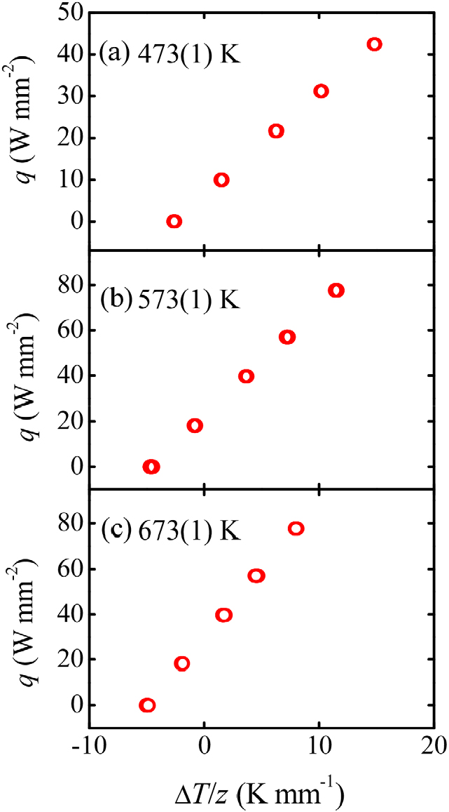
Fig. 3.
Heat flux (q) versus temperature gradient (ΔT/z) for the determination of thermal conductivity at 473 (1) K (a), 573 (1) K (b), and 673 (1) K (c). The q, which can be determined as Ri2 using the electric current (i) and resistivity of the heater (R), is observed for a heater attached to the top of a sample cut into square columns. The temperature gradient is calculated as the temperature difference (ΔT) between the thermocouples at the upper point and the lower point on the sample surface, divided by the distance (z) between the thermocouples. Our sample setting and measurement system has been reported in a literature.32) Temperatures denoted in the panels are averaged values during measurements for each point in a panel. It is noted that the averaged values are controlled for each point with different q and ΔT. About 2 hours are required for a measurement to obtain each point in a panel. Provided Stefan-Boltzmann law, a heat transfer between the sample surface (1) to the inner wall surface (2) for the equipment (Q’1→2) is equal to σSB ‧ A1F1→2 (T14-T24). σSB: Stefan-Boltzmann constant ~ 5.67 ‧ 10-8 Wm-2 K-4, A1: area for the sample surface ~ 1.5 ‧ 10-5 m2, F1→2: view factor from surface (1) to surface (2) ≤ 1, T1: temperature for surface (1) = temperature of the sample, T2: temperature for surface (2) > R.T. ~300 K. Maximum Q’1→2 yields ~ 0.179 W during this measurement.33) In a panel, “differences of Q’1→2” for each point should be observed as a deviation from linearity for a q-ΔT/z curve, although the deviation is not clearly observed for each panel. “Absence of the deviation” indicates that amounts of “differences of Q’1→2” are small enough for each measurement. In present results, we conclude that “differences of Q’1→2” are negligible to obtain thermal conductivities (κ) assuming Fourier’s law.34)
Fig. 4 shows the temperature dependence of ρ, κ, S, and ZT for the δ = 0.01 sample. The ρ is 6.8 ‧ 10-4 Ωm at 300 K, and ρ and S increases with increasing T. These normal transport properties indicate that LaCu1-δS0.5Se0.5O (δ = 0.01) is conventional degenerate semiconductor at T = 300~700 K. As shown in Fig. 4(b), the κ of the δ = 0.01 sample measured by steady-state method is 2.4 Wm-1 K-1 at 473 K, and it increases with increasing T. Other κ, which is obtained using laser flush method, is 1.7 Wm-1 K-1 at 463 K. The other κ also increases with increasing T. For the laser flush method, specific heat of the sample, which was measured simultaneously using a conventional relaxation method equipped in Ulvac TC7000 as an indirect measurement, increases with increasing T. Regardless of measuring methods, both κ demonstrate similar temperature dependence qualitatively. The κ obtained by the steady-state method was used to calculate ZT. As shown in Fig. 4(c), the S of δ = 0.01 sample is 37 µVK-1 at T = 473 K. The positive S indicates that the dominant carrier is the hole. As shown in Fig. 4(d), experimentally calculated ZT from these results was 3.1 × 10⁻⁴ at 473 K and the ZT increases with increasing T. The ZT reached 6.4 × 10⁻⁴ at 673 K.
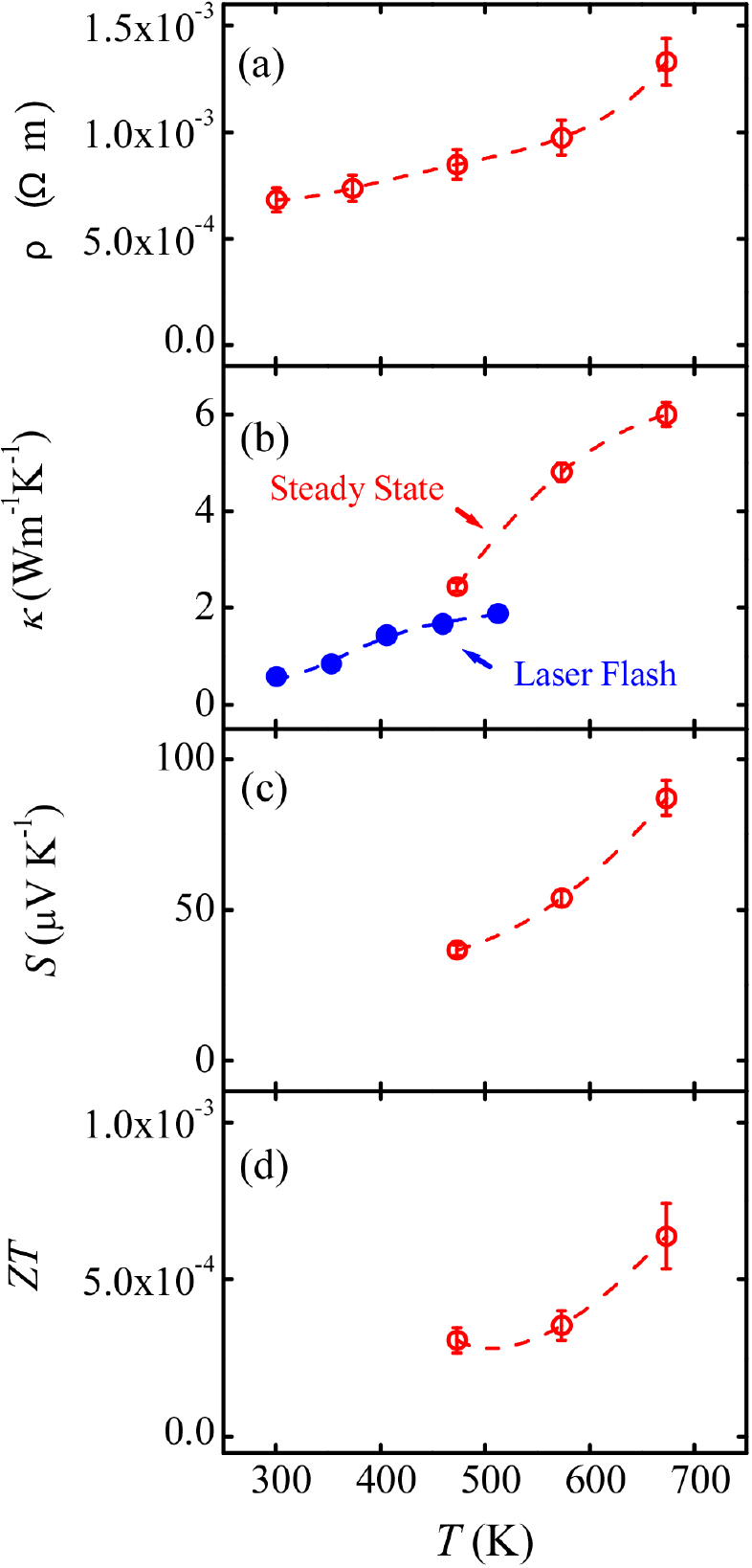
Fig. 4.
Electrical and thermal transport properties as a function of temperature (T) for LaCu0.99S0.5Se0.5O sample. (a) Electrical resistivity (ρ) versus T. (b) Thermal conductivity (κ) versus T. The red plot shows the steady-state method and the blue plot shows the laser flash method. (c) Seebeck coefficient (S) versus T. (d) Dimensionless figure of merit (ZT) versus T. The dotted line denotes expected data. We should point out such κ-T curve is not observed for a pure lattice without crystallographic defect. Further investigations are required for the thermal mechanism on a crystal with disordered crystallographic sites, although single crystalline samples and/or polycrystalline samples with the lower porosity are desirable for the further investigations.35)
3.2. Discussion
As shown in Table 1, the lattice constants of the δ = 0.01, 0.02 are smaller than those of a nominal LaCuS0.5Se0.5O which was reported by Ueda et al.11) in 2002. In Table 1, δ = 0.01, pure, weakly doped samples, which were defined in previous report, were prepared using a nominal chemical composition LaCuS0.5Se0.5O and different synthesis route and heat treatment temperatures. Although these nominal LaCuS0.5Se0.5O samples exhibit a larger lattice constants and lattice volume than those of Cu deficient samples, a quantitative chemical analysis and direct measurement on amount of the δ ~0.01 is still very difficult.
As shown in Fig. 4(b), κ of the δ = 0.01 sample exhibits quantitative differences values between steady-state method and laser flash method at T~ 473 K. The κ, which was measured indirectly using the laser flash method, showed 29 % lower than that of the κ measured directly using steady-state method. Such difference from measurement methods does not contradict with a systematic error, which was reported for the lower κ measured by laser flash (κLF) and the higher κ measured by steady-state method.36,37)
The difference can be attributed to various factors. Wang et al.38) reported κLF can vary by about 10 % due to the influence of the measuring instrument and the software used for measurement. Additionally, κLF depends on the anisotropy25,36) and heterogeneity36) of the sample. Systematic error also accumulated from measurements of a thermal diffusivity, a specific heat, and a density of the sample. In present thermal transport measurement using laser flash method, 10 % of the systematic error is probably due to the laser flash instrument and the software. 20 % of the systematic error can be attributed to other additional laser flash measurement uncertainties. Porosity and pore size of the sample may contribute to enhance systematic errors in both the steady-state and laser flash methods in different way.39) The sample size further affects the accuracy of measurements. To improve measurement accuracy, highly compacted samples are required.
We should comment on these transport and thermal properties in comparison with polycrystalline samples with different chemical compositions in LaCu1-δS1-xSexO series. Yasukawa et al.23) reported κLF = 2.1 Wm-1 K-1 at room temperature for an x = 1, nominal δ = 0 (undoped LaCuSeO) polycrystalline sample, in which porosity was 16 vol% without figures showing XRD patterns for their polycrystalline samples. Yasukawa et al.23) did not report on temperature dependence of κLF. While Yasukawa et al.23) reported the semiconducting ρ-T and metallic S-T curves for undoped LaCuSeO, Kato et al.25) reports semiconducting ρ-T and S-T curves for LaCuSeO with 9.6 vol% porosity.
In our present understanding, pure LaCuSeO is an insulator exhibiting optical band gap ~2.7 eV and ρ ~ 104 Ωm. Both results, which are reported by Yasukawa et al.23) and Kato et al.,25) indicate that their LaCuSeO samples contain slight copper defect resulting p-type carriers and semiconducting transport properties. Metallic S-T curve, which was reported by Yasukawa et al.,23) suggest heterogeneity of the polycrystalline sample. Therefore, we compare thermal properties between present La0.99CuS0.5S0.5O (δ = 0.01) and Kato et al.25)’s nominal LaCuSeO. Although the nominal LaCuSeO exhibits a typical κLF-T curve as a lattice at well above the Debye temperature, the present δ = 0.01 sample exhibits κ and κLF increasing with increasing T at T ≥ R.T. Such κ-T curve of the La0.99CuS0.5S0.5O is probably due to a randomness and/or defect of Cu sites qualitatively. At room temperature, κLF of nominal LaCuSeO with 9.6 vol% porosity are 2.47 and 3.06 Wm-1 K-1 depending on a pressing direction during hot pressing.25) On the other hand, κLF is ~0.7 Wm-1 K-1 for present La0.99CuS0.5S0.5O with 45 vol% porosity. It is noted that there is no report on κLF for nominal polycrystalline LaCuS0.5Se0.5O and we cannot compare simply between nominal LaCuSeO with 9.6 vol% porosity and La0.99CuS0.5S0.5O with 45 vol% porosity without thermal properties of nominal polycrystalline LaCuS0.5Se0.5O with clear porosity. Further comparison and discussion between nominal LaCuSeO and La0.99CuS0.5S0.5O are beyond our scope. It is also noted that there are no κLF for LaCuSO with clear porosity and κ at high temperatures, although Goto et al.16) reports that the value of κ is 2.3 (3) Wm-1 K-1 at 300 K. Goto et al.16) reports that the κ increase with decreasing T, indicating the κ-T curve predominantly via phonon-phonon Umklapp scattering40) as well as LaCuSeO.25) Provided that κ of LaCu0.99SO, which is reported by Goto et al.,16) exhibits κ-T curve simply extrapolated at T = R.T. - 673 K, κ-T curve of the La0.99CuS0.5S0.5O is qualitatively different from both of LaCuSO and LaCuSeO at T = R.T. - 673 K.
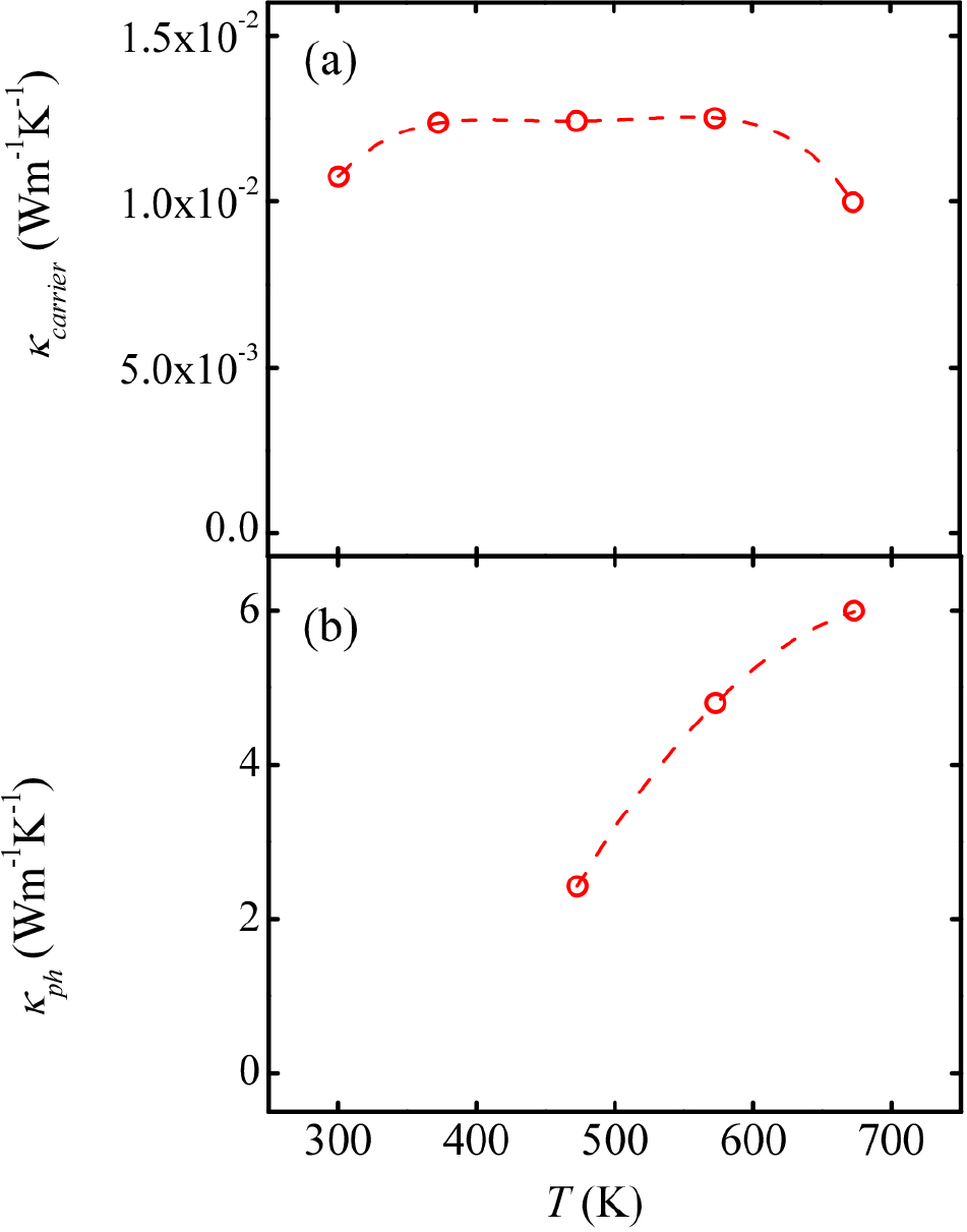
In a general simple assumption, κ of a conductor consists of contributions from carriers and phonons. To quantify the contributions of carriers and phonons to the thermal conductivity, carrier thermal conductivity (κcarrier) is estimated from Wiedemann-Franz law expressed as Eq. (1).
where, L is known as the Lorenz number. We used the value of 2.44 × 10⁻⁸ V2 K-241,42) at T = R.T. - 373 K, and we used the Lorenz number experimentally determined by Seebeck coefficient as 43) at T = 473~673 K. Estimated κcarrier is plotted as a function of temperature in Fig. 5(a). The κcarrier is generally constant between 373 K and 573 K, and it takes a maximum value at 573 K. This suggests a change which reduces the thermal conductivity and might be due to a displacement in a local structure in the unit cell at T > 573 K. As described in previous work,28) slight differences within 2 at% in the amount of copper defects cause the variety of the electronic properties of the material from insulating phase (δ = 0) to degenerate semiconducting phase (δ ~ 0.01) and other insulating phase (δ ~ 0.02). Provided a thermally activated displacement of copper defects, occurrence of one copper defect displacement in an approximately 5 × 5 × 5 unit cell will significantly affect the transport properties and possibly results thermal hysteresis in the ρ-T measurements, although such a hysteresis has not been observed clearly in the present report. The anomalous maximum of κcarrier might be an indication of the possible displacement of copper defect at T > 573 K.
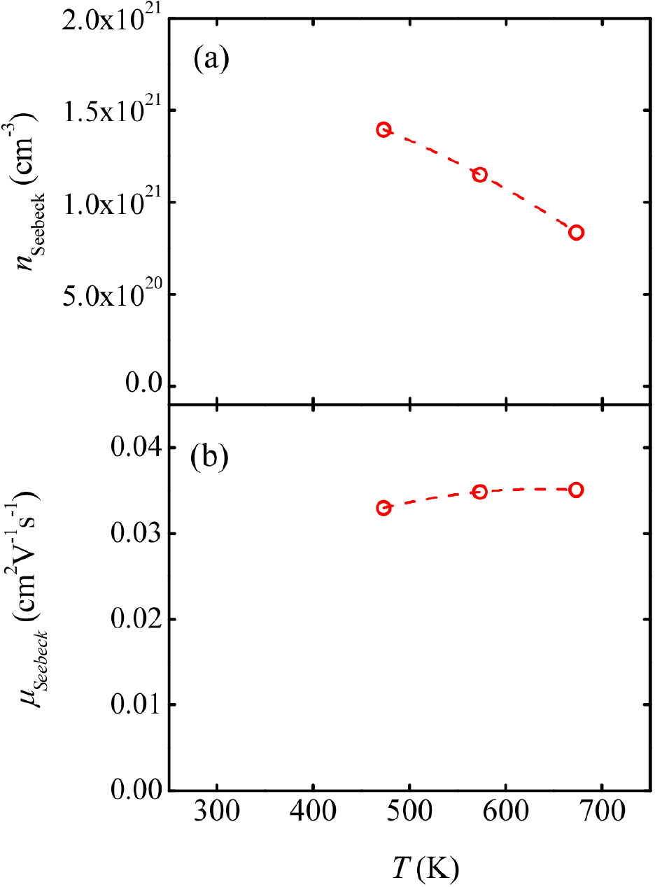
Fig. 5(b) shows a phonon thermal conductivity (κph) as a function of temperature, which is obtained by subtracting carrier thermal conductivity from the total thermal conductivity (κ). The κph accounted for more than 99 % of the κ. Provided a simple metallic thermoelectric power for a quasi 2D Fermi-liquid system like normal conducting phase in analogy for copper-based high-Tc superconductors, a temperature dependence of carrier concentration can be calculated from Seebeck coefficient. In the lowest order approximation, S is expressed as functions of the carrier concentration (nseebeck) as Eq. (2).
where, dc (8.66 Å) is the interlayer spacing, e (>0) is the unit charge, and m* is effective electron mass.44) Carrier mobility (µSeebeck) can also be estimated from the calculated carrier concentration. As shown in Fig. 4(c), the experimental S-T curve exhibits a larger |S|, which is not simply interpolated using the Eq. (2), at a higher temperature. The larger |S| is probably due to the decreasing of the carrier density at the higher temperature. Although a direct measurement of the carrier density verified using Hall effect exceeds our scope, such a negative temperature dependence of the carrier density is reported at T > 200 K for Mg-doped LaCuSeO thin film.15)
The effective mass ratio can be theoretically calculated by applying a parabolic approximation to the band structure results obtained from density functional theory (DFT), and then differentiating the interpolated differentiable curve twice to obtain the reciprocal of the coefficient. Experimentally, the effective mass ratio can be determined using certain models. For example, Lan et al.45) derived it by setting up a model for Hall mobility and Seebeck coefficient. Hiramatsu et al.46) optically determined it for the binary system CuSe. For Mg-doped LaCuSeO, Hiramatsu et al.47) determined the effective mass to be 1.6 me (where me is the mass of an electron) from transport phenomena.
Since the Hall effect of the material has not been measured, we adopt the value of Mg-doped LaCuSeO determined by Hiramatsu et al.47) as a provisional measure. The interlayer spacing is defined as the c axis length of this material, which is a layered structure.
Fig. 6 shows the temperature dependence of nseebeck and µSeebeck. The nseebeck is calculated as ~1021 cm-3. Such a large nseebeck is often observed in mixed anion layered compounds.48) In fact, Hiramatsu et al.15,47) have also reported n on the order of 1020~1021 cm-3. The temperature dependence of the nseebeck does not contradict with the results presented by Hiramatsu et al.47)
As shown in Fig. 5 and Fig. 6, nseebeck decrease with increasing temperature, and µSeebeck is almost constant regardless of temperature, while the κ increases with increasing temperature. In an ideal lattice, a phonon thermal conductivity is inversely proportional to T at T > ~300 K, although the κ increases with increasing T for LaCu0.99S0.5Se0.5O.
It should be admitted that the discussions must be limited in phenomenological approach and qualitative approach on the κ-T curve. Because a quantitively analysis and further physical refinement should be made on thermal properties for bulk single crystalline samples without second phases or hot-pressed polycrystalline samples with the lower porosity at larger temperature regions. So following sentences describe our speculations and related physical constants for research in a future.
In a phonon-gas model,49) phonon thermal conductivity can be expressed as Eq. (3).
where, (C, , and l) are (a heat capacity, an average velocity of sound, a mean free path). Since l of an ideal lattice is proportional to T-1, an ideal κph decreases with increasing T at well above the Debye temperature.49) On the other hand, for LaCu0.99S0.5Se0.5O, assuming that the S0.5Se0.5 site is chemically disordered, the Cu defects may increase the phonon scattering probability as a real-space factor. Thus, the effective mean free path is expected to be dominated by the shorter one of the intrinsic mean free paths (λ) and a characteristic scale parameter (D) determined by randomly doped S/Se site and Cu defects. For imperfect crystals and glasses, we predict a small constant conductivity at high temperatures, and l ∝ T-2, κ ∝ T at high temperatures when a dominant phonon length ~λ exceeds the D. Indeed the κph increase with increasing T for LaCu0.99S0.5Se0.5O. Further, the thermal conductivity will have an upward convex relationship with a maximum at T where λ = D. It is noted that this upward convex relationship in thermal conductivity is not unique to LaCu0.99S0.5Se0.5O. Thermal conductivity of Cu1.8-2xBi2xS1-3xSe3x,50) Cu2-xS,51) Cu1.8S1-xTex52) and Cu2-xSe0.5S0.553) measured by the laser flash method show similar trends. Additionally, according to the Debye model for a lattice without randomness and defects, the thermal conductivity of a pure metal is expected to decrease with increasing temperature at T > ~300 K, while thermal conductivity increases with temperature above 300 K in Bi2Te3,54) Bi2Te2⋅5Se0.555) and Bi2Te2.7Se0.356) measured by laser flash method, although the detailed mechanism of these thermal properties is still unknown.
4. Conclusion
LaCu1-δS0.5Se0.5O polycrystalline sample with Cu deficiency (δ = 0.01) was prepared and its dependence of transport properties was measured. Electrical resistivity of the sample with δ = 0.01 is one part per million than that of pure sample (δ = 0) at room temperature, although ZT of δ = 0.01 is very small. Thermal conductivity of the sample with δ = 0.01 increases with increasing T at T > ~300 K. This thermal property is different from pure lattice without crystallographic defect, while this thermal property is similar to several TEC materials.


