

1. Introduction
2. Theoretical Part
2.1. Structural properties
2.2. Electrical properties
3. Experimental Part
4. Results and Discussion
5. Conclusion
1. Introduction
Superconductivity remains the greatest hope for modern technology to advance ways to reduce energy and electricity consumption. The phenomenon of superconducting conductivity occurs when the resistance is zero and by using cooling and reaching the critical temperature or the transitional temperature, many characteristics distinguish superconducting materials, including the critical of magnetic field (Hc), temperature T(c) and the critical current density Jc, when any increase or decrease in any property occurs, the material returns to its first state without being superconductor. Bi-base is a superconductor that has three phases Bi-2223, Bi-2201, and Bi-2212, the last two combinations are known for their great research properties and essential uses in technology and industries.1-5) There is a search-prepared diffraction analysis of X-ray showed the two phases Bi-2223 and (Bi,Pb)-2212 coexist in samples with a rhombic crystal structure. The critical initiation temperatures Tc(offset) and the zero resistance critical temperatures Tc(onset) were determined from DC electrical resistivity measurements by phase determination and microscopic samples characterization were examined by SEM and XRD. Moreover, measurements of DC electrical resistivity as a function of the critical current density (Jc), temperature, AC magnetic susceptibility and measurements of DC magnetization were performed to evaluate the samples relative performance.6) BBCCO is formed from bismuth oxide, barium oxide, calcium oxide, and copper oxide which is glass of materials ceramics. They are non-metallic and inorganic materials that are produced by cooling or heating. This material has many excellent properties, including hardness, temperature tolerance, corrosion resistance, low thermal and electrical conductivity, and resistance to bending. Investigations were made and it was found that the system of Bi-Sr-Ca-Cu-O has a high degree of superconductivity at high temperatures.7-9) X-ray diffraction analysis performed as part of the research showed that the two phases of Bi-2212 and (Bi,Pb)-2223 coexist in samples with rhombic crystal structures. The initiation critical temperatures (Tc onset temperatures) and the critical temperatures for zero Tc electrical resistance (R = 0) were determined from DC electrical resistance measurements by phase determination, and the microscopic properties of the samples were examined by SEM and XRD. In addition, continuous measurements of resistivity as a function of the temperature, AC current are possible and critical current density Jc. DC magnetization measurements and magnetic susceptibility were performed to evaluate the relative performance of the samples. It has been established that all the physical properties of these materials change with the phase change, the way they are manufactured and the type of chemical elements included in their composition.10)
Research in engineering and ceramics has become an essential field to rise critical temperatures for these materials, and researchers have continued developing new ceramics types.11) The researches reference,12) the superconducting dibasic ceramic compound Bi2Ba2Ca2Cu3O10+δ was prepared with different pressures of 5, 7, and 9 tons/cm2, and the structural and electrical properties of this compound were investigated, it was found that the electrical and structural properties, changes by increasing pressure. The electrical and structural properties of the compound Bi2-xPbxSr2Ca.2Cu3O10+δ were studied at a pressure of 8 tons/cm2 and a temperature of 855~860 K for 72 h and it was found that the transition temperature increases by 106~131 K 113~138 K, with an increasing proportion of lead replacing bismuth, and the structure is rhombic and phased 2223, and the intensity was found to increase with an increasing proportion of lead.13) In this paper, we will prepare compounds Bi2Ba2Ca2Cu2.9Ni0.1O10+δ, Bi2Ba2Ca2Cu2.8Ni0.2O10+δ and Bi2Ba2Ca2Cu2.6Ni0.4O10+δ compounds and studied the partial replacement of the copper with nickel and its effect on physical properties.
2. Theoretical Part
2.1. Structural properties
The X-ray examination is concerned with the study of materials as well as structural transactions using many scientific solutions. It is also interested in knowing the distance between atoms.14) The FWHM, Crystallinity (β), and strain were calculated as well as the crystallite size was calculated by comparing the modified Scherer and Scherer methods and comparing it with the Williamson-Hall method (DS, DS. Mod. DW-H), after which the dislocation density (δ) and microstrain (ƹ) were calculated all this using an X-ray diffraction.15)
Scherer’s method is a method for analyzing XRD according to the formula for calculating the crystallite size of a crystal:16)
where, DS (nm) is the crystallite size by Scherer, θ is Bragg’s angle in radian unit, K is the factor of Scherrer ≈ 0.9, λ refer to X-ray wavelength = 1.54060 Å, β is a line broadening at full-width half maximum peaks in radian unit.
The Williamson-Hall method is the easiest-to-use method for finding crystal size (DW-H) and strain (ƹ) from the Eq. (2).17,18)
ϐ: The crystallinity in percentage, DWH is the crystallite size by Williamson Hall.
The area of the crystalline peaks is the area under the amorphous void (represented by crystalline peaks area), all peaks area is the crystalline peaks (represented by crystalline peaks and the area of amorphous).17)
Under the influence of annealing temperature on the dislocation density and microstrain were measured as a result of X-ray diffraction from Eqs. (4) and (5):18,19)
where, δ is the dislocation density in nm-2, D is crystallite size by Scherer, ε is the microstrain, β is the FWHM = Full-Width Half Maximum.
2.2. Electrical properties
The electrical properties of the samples were examined using the four probes technique to measure the resistivity from Eqs. (6) and (7):20-23)
where, R (Ω) is the electrical resistance, A (cm2) is the area, L (cm) is the length of specimens.
The electrical resistance completely disappears when the superconducting materials are cooled to a certain temperature to determine the zero resistance transition temperature, and the transition temperature is different from the Eq. (8):
Then used the Eq. (9) to calculate the energy gap:
where, Eg is the energy gap in electron volt, Kb is Boltizman constant = 1.38 × 10⁻²³ J/K.
3. Experimental Part
The Bi2Ba2Ca2Cu3-xNixO10+δ compounds with X values are 0.1, 0.2 and 0.4 were prepared by a standard solid-state reaction (SSR) method from element oxides (Bi2O3, BaO, CaO, CuO and NiO), pure state of the compound Bi2Ba2Ca2Cu3O10 was not taken because it was studied at different sintering temperatures (810, 830, 850, 870, 890) °C and showed that the sample prepared with sintering temperature 850 °C. Then the properties of the lattice parameters a = b ≠ c were calculated.24) But in this research, the oxides powder will be weighed using the Electronic Balance type KERN-4 digits, and their proportions are calculated according to the chemical Eq. (10):
Then the oxides were mixed using agate mortar, the powder was ground for 1 h with a Vortex Mixer, and dried in an automatic electric furnace at 100 °C for half an hour. The samples were pressed by a MEGA hydraulic press at a pressure of 7 (ton/cm2). In the final step, the samples were sintered in a Carbolite CWF 1200 furnace at 860 K for 192 h and cooled to room temperature as the researchers did in their research before.24) Study of the crystal structure of samples using (the Shimadzu Lab XRD-6000 device), crystallization, crystallite size, dislocation density, and macrostrain by comparing the Scherrer method with the Scherrer modified method and Williamson-Hall method. After that the electrical properties as shown by drawing a relationship between temperature and resistivity (T-R) to measure the resistivity.
4. Results and Discussion
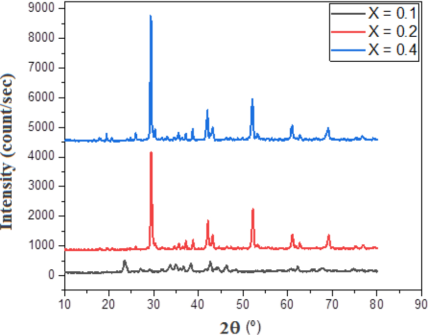
The samples pattern of the X-ray diffraction were taken for this different partial substitution for all Bi2Ba2Ca2Cu3-xNixO10+δ samples, as shown in Fig. 1 while representing the relationship between the Bragg angle and intensity for three existing models.
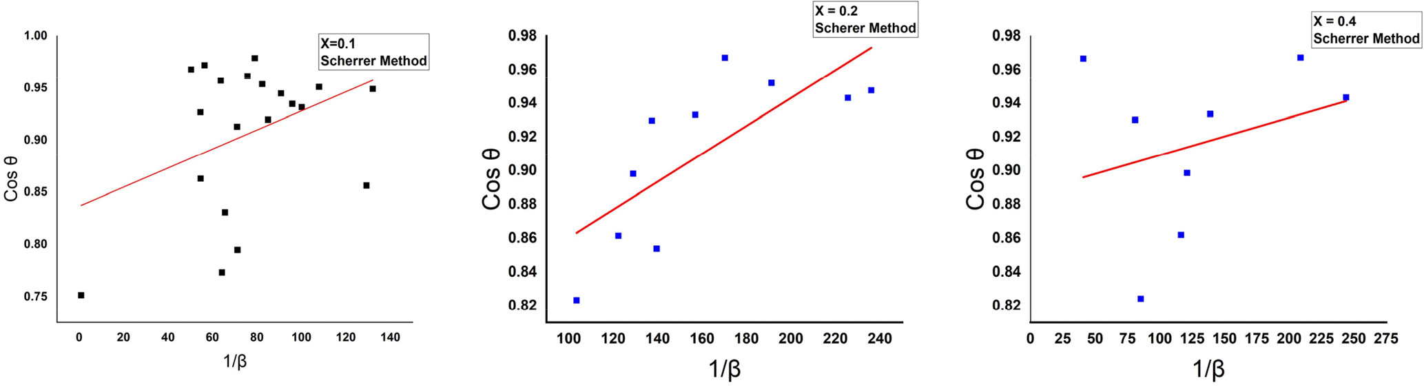
The relationship between 1/β in the X-axis, Cos θ in the Y-axis in the Scherrer method, and drawing the best straight line by using the origin 2019b program and the slope of the curve to calculate the crystallite size, as shown in Fig. 2.
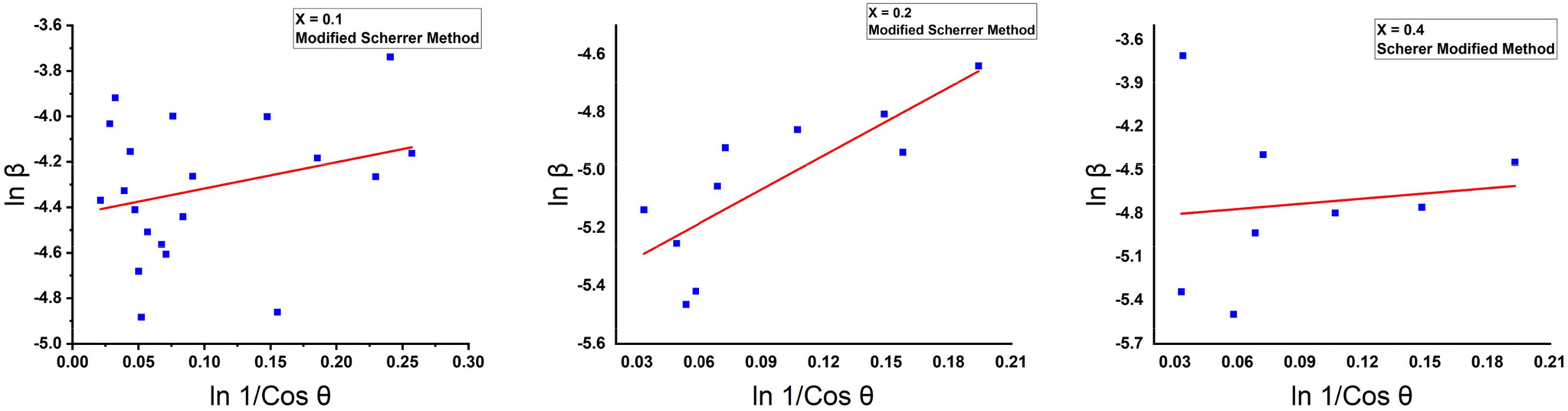
The relationship between ln β in the X-axis, ln 1/ Cos θ in the Y-axis in the modified Scherer method, and drawing the best straight line by using the origin 2019b program and the slope of the curve which represents the microstrain was calculated the crystallite size, as shown in Fig. 3.
The relationship between the 4sinθ in X-axis, β Cos θ in Y-axis in the Williamson-Hall method, and drawing the best straight line by using the origin 2019b program and the slope of the curve which represents the strain was calculated the crystallite size, as shown in Fig. 4.
From all the above methods analysis prepare result as shown in Table 1.
Table 1.
Results of crystallite size, macrostrain, dislocation density, and FWHM by using Williamson-Hall methods and in Scherrer method, and Scherrer modified method.
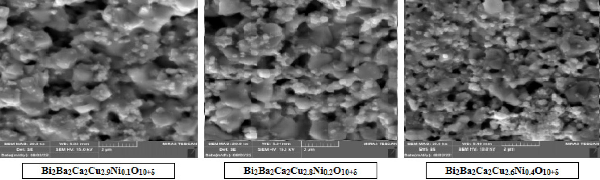
The structure (morphology) of the three phases was examined using the (SEM) technique at an amplification of 20.0 KX, it was found that the size of the granular forms exceeds 25 nm. It has been determined that as the concentration of nickel increases, the samples’ shape changes. In addition to having distinct homogeneity in the patterns and having light and dark areas that show where the crystal structure is distributed. As demonstrated in Fig. 4, the tests reveal a change in size, the production of new phases, and tiny granular sizes. A drop in granule size results in an increase in the number of granules, which in turn helps to increase the granular area.25,26)
From examining the electrical properties, the critical temperature was calculated by drawing the relationship between the resistivity and temperature in Kelvin units, as in Fig. 5.
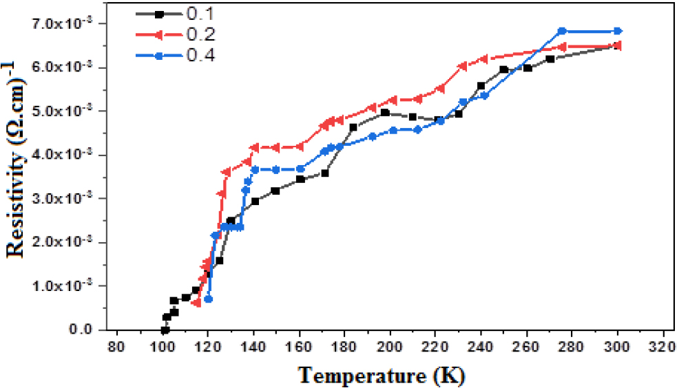
We note in the results Table 4 that the three samples had a metallic behavior and we noticed an increase in the resistivity with the increase in temperature. Table 2, illustrated all results of crystallinity, The area of crystalline peaks, the area of all peaks, and FWHM. While the gained results from the mentioned relations are shown in Table 3.
Table 2.
All results of crystallinity, The area of crystalline peaks, the area of all peaks, and FWHM.
| Number of samples | Crystallinity % | The area of crystalline peaks | Area of all peaks | FWHM |
| 1 | 0.98 | 5958.15 | 6067.1 | 0.0837 |
| 2 | 0.59 | 4291.5 | 7274.45 | 0.0066 |
| 3 | 0.5 | 3917.9 | 7768.8 | 0.0101 |
Table 3.
Dislocation density, microstrain, and d-spacing.
Table 4.
The value of Tc onset, Tc offset, and the energy gap (Eg).
| Partial substitution | Tc onset (K) | Tc offset (K) | ΔT (K) | Eg (ev) × 10-21 |
| 0.1 | 170 | 100 | 135 | 6.57639 |
| 0.2 | 140 | 118 | 129 | 6.28411 |
| 0.4 | 134 | 120 | 127 | 6.18668 |
The resistivity decreased slowly from 300 K to the temperature at which the samples transform from the normal state to the superconducting state Tc(onset) after those temperatures the resistivity of the samples rapidly declines begins to zero at the critical temperature Tc(offset). When substitutional nickel at a partial substitution ratio of 0.1 instead of copper, the temperature began to decrease gradually from 300 K, then the decrease suddenly became 125 K, then when adding nickel at a partial substitution ratio of 0.2, the temperature began to decrease gradually from 300 K then the decrease suddenly became at 122 K, while in the last sample, when adding Ni at a partial substitution ratio of 0.4 instead of Cu, the temperature decreased gradually, starting from 300 K, then it suddenly decreased at a temperature of 120 K, all these changes of increase and decrease due to the change in the composition of the compound when changing the ratio of nickel substitution,26) and this leads to a change in the distances between the Cu-layer with another Cu-layer, and this reason is very important in superconductivity as this distance depends to Cooper’s pairs, as it happened in the search.27)
5. Conclusion
This search focuses on the study of copper partially replaced by nickel Bi2Ba2Ca2Cu2.9Ni0.1O10+δ, Bi2Ba2Ca2Cu2.8Ni0.2O10+δ and Bi2Ba2Ca2Cu2.6Ni0.4O10+δ compounds by the method of solid-state reaction. The DC electrical properties were studied by the four-point probe technique to determine a critical temperatures samples and to know the partial replacement effect of Cu with Ni. It was found that both the energy gap and critical temperatures are slightly affected by partial replacement. Where it was obtained critical temperature, Tc(offset) = 100 K at the first sample, and in structural properties the same sample has a low measure in crystallite size in Scherrer equal to 97.230 nm, Scherrer modified equal to 116.678 nm with strain equal to 1.15466, and the crystallite size in Williamson Hall methods equal to 119.887 nm with strain -1.67756 × 10⁻⁴. according to an analysis of the structural morphology of the phases using (SEM) technology. It has been established that the form of the samples alters with nickel concentration. In addition to showing noticeable homogeneity in the patterns that depict the distribution of the crystal structure and size of the granular forms surpassing 25 nm.
