

1. Introduction
Transparent conducting electrode(TCE) films with wide energy band-gaps(Eg) are intensively studied, to be used with various optoelectronic devices operating at the ultraviolet( UV) wavelength range, such as photovoltaic cells, detectors, sensors, and light emitting diodes.1,2) While the TCE films are required to have both of the low resistivity and the high transmission,3) it is generally observed that the resistivity values of the TCE films drastically increase when their Eg values are increased.4-6) Basically, as the Eg of a TCE film increases, the carrier mobility and/or the carrier concentration decrease due to the increase in the effective mass of the free carriers and/or the degradation of the crystalline quality.4-6)
Recently, ZnO films co-doped with Mg and Be(Zn- MgBeO films) have attracted attention as one of the promising TCE materials for the UV-range optoelectronics, as their Eg values can be continuously modulated from 3.7 to 4.9 eV by changing the concentration of MgO and BeO.7) It has been also reported that the electrical properties of the ZnMgBeO films may be improved by adding Ga donor atoms and the optimized Zn0.88Mg0.05-Be0.03Ga0.04O films show excellent transmission properties, with an Eg of 3.75 eV. Unfortunately, its resistivity is still quite high, ~1.6 × 10⁻³ Ωcm, and needs to be improved.8)
It has been reported that the oxide/metal/oxide multilayer films, such as ZnO/Ag/ZnO, AlZnO/Ag/AlZnO, GaZnO/Ag/GaZnO, ZnMgBeO/(Cu)/Ag/ZnMgBeO, InSnO /Ag/InSnO and TiO2/Ag/TiO2, show much improved electrical properties while maintaining the high transmission.9,14) A resistivity of ~ 5 × 10⁻⁵ Ωcm and maximum transmittance of higher than 85 % have been reported to be obtained by inserting a thin Ag film between the oxide films.13)
In this work, Ag thin films with thickness of 5~20 nm were inserted between two layers of ~20 nm thick Zn0.88-Mg0.05Be0.03Ga0.04O films, in an effort to improve the electrical properties of the ZnMgBeGaO film. Optical and electrical properties of the resulting multi-layer structures were characterized in detail, utilizing the Hall measurements, the four-point probe the UV-Vis spectrophotometer analyses, and the transmission electron microscope (TEM). Effects of annealing treatment on the properties of the multilayer structures were also investigated.
2. Experimental
The Zn0.88Mg0.05Be0.03Ga0.04O/Ag/Zn0.88Mg0.05Be0.03Ga0.04O layers were grown on quartz substrates by radio frequency( RF) sputtering at room temperature. A sputter target of ZnMgBeGaO containing 5 at.% MgO, 3 at.% BeO and 4 at.% Ga2O3 was used for the oxide layer and pure Ag target was used for the metal layer. The sputtering chamber was initially evacuated down to a pressure of 10−3 Pa and then, the chamber pressure was maintained at 0.67 Pa during the sputtering process by flowing Ar gas. The RF power of process deposited oxide layers and Ag layer were fixed at 75W and 30W, respectively. The thickness of each layer was controlled, depending upon the process condition used to grow the film. Some of the samples were post-annealed at temperatures ranging from 100~300 °C in vacuum of 10−3 Pa for 20 minutes.
The electrical properties such as sheet resistance, resistivity, carrier concentration and mobility were characterized by a 4-point probe system(Changmin Tech, CMTSR2000) and a Hall measurement system(M/N #7707_ LVWR, LAKE SHORE CRYOTRONICS INC., USA) operated at room temperature. The optical transmittance of the deposited films was recorded using an UV-visible spectrophotometer(VARIAN Technologies, USA). The calibration of the spectrophotometer was performed against a quartz substrate as a reference before measurement and the absorption coefficient was obtained from the transmittance curve. The thickness of the films were evaluated by a transmission electron microscope(TEM, JEOL JEM 2000FX) operated at 200 kV.
3. Results and Discussion
Fig. 1 shows effects of Ag layer thickness(tAg) on the electrical properties of the Zn0.88 Mg0.05Be0.03Ga0.04O(20 m)/Ag(0~20nm)/Zn0.88Mg0.05Be0.03Ga0.04O(20m) multilayer structures. It is observed that the 60 nm thick ZnMgBe- GaO film(tAg = 0 nm) shows a high electrical resistivity, ~ 1.6 × 10⁻³Ωcm. When an Ag layer film is placed between the two ZnMgBeGaO films, the resistivity drastically decreases to ~4.0 × 10⁻⁵ Ωcm for the 10 nm Ag and ~1.4 × 10⁻⁵ Ωcm for the 20 nm Ag. The carrier concentration increases by about two orders of magnitude and the Hall mobility of the multilayer increases with increasing Ag thickness(from 3.7 × 1020 cm−3 and 7.8 cm2/ V.s for 0 nm tAg to 4.1 × 1022 cm−3 and 10.4 cm2/V.s for 20 nm tAg). It is noticeable, however, the significantly low mobility is observed in the case of the 5 nm thick Ag interlayer, 2.3 cm2/V.s.
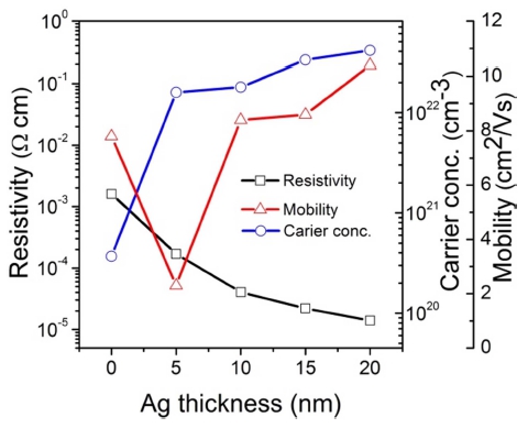
Fig. 1
Electrical properties of the ZnMgBeGaO/Ag/ZnMgBeGaO multilayer structure as a function of Ag layer thickness.
Fig. 2 shows the transmittance curves of the multilayer structures as a function of the Ag thickness. It is observed that the transmittance decreases with the Ag insertion, which is more evident at the long wavelength(λ) region. Notice that the transmission at 700 nm wavelength decreases from 91 % at tAg = 0 nm to 76 % at tAg = 10 nm and 28 % at tAg = 20 nm, whereas the transmission at 550 nm wavelength changes from 90 % at tAg = 0 nm to 94 % at tAg = 10 nm and 57 % and tAg = 20 nm. The transmission also abnormally decreases in the case of the 5 nm Ag sample. It is seen that the multilayer structure with 10 nm Ag shows reasonable transmission, higher than 85 % at λ = 380 nm ~ 640 nm and 65 % at λ = 640 nm ~ 780 nm.
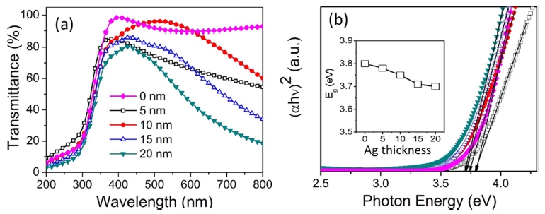
Fig. 2
Optical properties of the multilayer structures as a function of the Ag layer thickness, (a) transmission spectra and (b) optical band gap.
It is believed that the resistivity of the ZnMgBeGaO/ Ag/ZnMgBeGaO decreases with the Ag insertion because the Ag layer provides a high number of charge carriers as well as the effective path to deliver the current, enhancing both the carrier concentration and the mobility.15) The transmittance of the multilayer structure decreases with increasing tAg, due to the reflection of light at the Ag/oxide interface and absorption by the Ag layer.15) It is believed that the transmission is more significantly deteriorated at the long λ range than at the shorter one, because the effect of Ag thickness on the refractive index of Ag films is less significant in the short λ range than in the long λ range. It has been reported that the refractive index of Ag changes from 2.8 for tAg = 6 nm to 0.2 for tAg = 12 nm at 700 nm, but from 0.7 for tAg = 6 nm to 0.3 for tAg = 12 nm at 380 nm.16)
It is observed that the carrier mobility(Fig. 1) and the transmission(Fig. 2) are more critically reduced at tAg = 5 nm. It is believed that this is because the Ag layer is not perfectly continuous at this thickness, resulting in very rough Ag/oxide interfaces and the irregular surface morphology, as seen in Fig. 3, cross-sectional TEM images of the ZnMgBeGaO/Ag/ ZnMgBeGaO samples. It is clear that a partially continuous film with rough interfaces was grown in the case of the 5 nm Ag sample whereas a continuous and relatively smooth film was in the case of the 10 nm Ag sample. The surface roughness was 0.8 nm and 0.4 nm for the 5 nm and the 10 nm samples, respectively, as measured by the atomic force microscopy. Obviously, films with the irregular shapes would scatter the incoming light as well as the traveling electrons, resulting in the low transmission and carrier mobility. This observation is consistent with the previous reports on the ZnO/Ag/ZnO and the ZnMgBeO/Ag/Zn- MgBeO multi-layer structures,15,17) that a transition point occurs from continuous films to island structures below a critical Ag layer thickness and the physical and optical properties of Ag differ considerably from those of the bulk material.
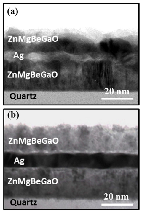
Fig. 3
Cross-section TEM micrographs of the ZnMgBeGaO/Ag/ ZnMgBeGaO multilayer structures with the Ag layer thicknesses of (a) 5 nm and (b) 10 nm.
In the inset box of Fig. 2(b), it is observed that the optical band gap energies of the multilayer structures decrease with increasing Ag thickness, from ~3.80 eV for tAg = 0 nm to ~3.70 eV for tAg = 20 nm, estimated using the Tauc’s relationship. It is believed that this is due to the “many-body optical band gap shrinkage effect”.15,18) As some of the electrons are injected from Ag layer into the conduction band of the ZnMgBeGaO layers, Ag atoms in the adjacent Ag layer may ionize partly and become positively charged. The electrical field between the positively charged Ag atoms and electrons in the conduction band of the ZnMgBeGaO layer causes upward shifting of the valence band and downward shifting of conduction band, resulting in an optical band gap shrinking.15,18)
Fig. 4 shows the transmittance and the resistivity of the ZnMgBeGaO(20nm)/ Ag(10nm)/ZnMgBeGaO(20nm) layer annealed in vacuum at various temperatures. It is seen that very little changes are observed in the transparency, but the resistivity sizably decreases with the increase of annealing temperature. The lowest resistivity of ~2.6 × 10⁻⁵ Ωcm(sheet resistance of 4.4 Ω/sq) is obtained at 300 °C which is ~35 % lower than that of the untreated sample. It is believed that the annealed multilayer structures have better microstructures with improved crystallinity, leading to the improved conductivity.19,20)
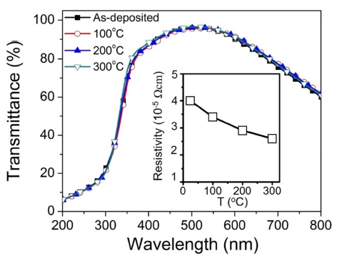
Fig. 4
Transmission spectra of the multilayer structures as a function of the annealing temperature. The inset box shows resistivity of the multilayer structures after annealing.
It is stated at this point that the ZnMgBeGaO(20nm)/ Ag(10nm)/ZnMgBeGaO(20nm) optimum structure studied in this work, with a resistivity of ~2.6 × 10⁻⁵ Ωcm, optical transmittance of 65 % ~ 95 % over the visual range, and the optical Eg of 3.75 eV, represents sizable improvement in terms of the electrical resistivity over the previously reported ZnMgBeGaO layer (with a resistivity of 1.6 × 10⁻³ Ωcm)8) and the conventional ITO films (with a typical resistivity of 2 × 10⁻⁴ Ωcm).21) The optimum structure also represents a significant improvement over the previously reported ZnO-based transparent conducting multi-layer films such as ZnO/Ag/ZnO, AlZnO/Ag/AlZnO, and GaZnO/Ag/GaZnO (with 50 % ~ 90 % transmittance over the visible range, Eg of ~3.2 eV, and resistivity of 5 × 10⁻⁵ Ωcm),11,15) especially in terms of the transmission at the short wavelength range.
4. Conclusion
The ZnMgBeGaO(20nm)/Ag(0~20nm)/ZnMgBeGaO(20 nm) multilayer structures have been sputter deposited on quartz substrates. The results indicate that the electrical resistance and the optical transmission substantially decrease with increasing Ag layer thickness. The multilayer structure with the optimum Ag thickness of 10 nm showed a resistivity of 4 × 10⁻⁵ Ωcm, the optical transmittance of 65 % ~ 95 % over the visual range, and Eg of 3.75 eV. Structures with thicker Ag films showed further improved electrical conductivity but much lower optical transmission. The multilayer structures with 5 nm thick Ag layer showed abnormally deteriorated properties, as the 5 nm Ag film showed partly discontinuous morphology with rough interfaces and surfaces. It was also observed that the electrical properties was improved by about 35 %, to the resistivity of 2.6 × 10⁻⁵ Ωcm, by the annealing in vacuum at 300 °C. The high conductivity as well as the reasonable transmittance of the ZnMgBe GaO/Ag/ZnMg- BeGaO multilayer structures indicate that they are promising candidates for the UV optoelectronic applications.
