

1. Introduction
In order to design modern optoelectronic devices like light-emitting diodes, solar cells, and photodetectors, it is essential to have a solid understanding of the interactions that take place between photons and electrons.1-4) As a result, the search for a high-performance photosensor has grown more pressing, and not just in terms of effectiveness, bandwidth efficiency, and speed; it also has to be productive across a large area, and it needs to integrate its technologies. 4-8) Due to the rapid development of integrated circuit technology and the material’s outstanding compatibility, single-crystalline silicon is the material of choice for the creation of photodetectors almost everywhere.9,10) Nevertheless, Si-based p-n junction devices continue to have a number of drawbacks, the most notable of which are their limited adaptability and poor photoresponsivity.11-14) Designing a Schottky junction with a suitable metal/ semiconductor combination, which efficiently provides a strong electrical field at the interface to capture photogenerated carriers, can eliminate most of these challenges.9,15) The metal electrode used in the Schottky junction can reflect light strongly, and thus the Schottky junction prepared with metal nanowires can be a suitable solution for a higher performing photosensor because it provides high optical transmittance and good electrical conductivity.
Note that a quasi-Fermi level splitting is probably caused by immediate photon illumination, which is known to cause the photogenerated direct current photovoltaic effect. Recent research has also shown that the sudden splitting and realignment of the quasi-Fermi levels for the electrons and holes in a junction causes a difference in potential between the two ends of the material.16-18) This difference in potential is what causes the sharp peak when the light is on and off, which is called the alternating current photovoltaic effect (ACPV).19) By coupling the ACPV with the built-in potential, its forward approach has the ability to alter the electron transport that takes place throughout the optoelectronic processes, resulting in a high-performing photodetector. However, the ACPV effect has not yet been utilized for photocarrier generation and separation through the use of a Schottky junction.
In this study, we made use of the photo-induced alternative photocurrent phenomenon, also known as “ACPV effect,” to develop a self-powered, ultrafast, and broadband (365 to 940 nm) photodetector. By exploiting the AC PV effect, the photoinduced current across the AgNWs/Si device can be boosted from 33 to 47 μA under selfpowered conditions. Ultrafast photoresponse of 36 μs for the rise and 382 μs for the decay durations is demonstrated by this photodetector.
2. Experimental
2.1. Device preparation
It promotes RCA cleaning to remove organic matter and contaminants on the surface of n-Si. In the case of RCA cleaning, acetone, isoprophenol, and DI water are given in this order for 5 minutes each. After cleaning, blowing is advanced using N2 to remove and give diwater remaining on the surface. After proceeding with blowing, HF treatment is performed to remove and give the natural oxide film SiO2 on the surface of n-Si. In the case of HF, a mixed solution of 100 mL of di-Water mixed with 1 mL of Hf was used. After HF treatment, di-water is used to rinse the remaining HF on the surface. Silver nanowires (AgNWs) is applied using a back dropper from which the natural oxide film SiO2 has been removed. In the case of AgNWs, it will apply about 0.2 mL of solution. After applying AgNWs, the AgNWs harden well, so they will be heat-treated at 60 degrees for about 20 minutes on the hot plate.
2.2. Electrical characterization and photoresponse.
A probe station was used to confirm the electrical characteristics. Hungk of Probstation makes contact on the part where AgNWs is applied, and in the case of the remaining one pole, it makes contact on the surface of n- Si where AgNWs does not rise. It illuminates various light-emitting diode (LED) sources from 365 to 940 nm on the part where AgNWs are applied. A function generator was used to adjust the wavelength of the LED. At first, it measures from -1 V to 1V with the LED turned off and dark. Next, the measurement is performed while gradually increasing the light intensity. With 0 V bias applied, it illuminates LEDs of various wavelengths from 365 to 940 nm and measures photocurrent.
3. Results and Discussion
To create a Schottky junction, a conventional AgNWs solution was applied and spread on a n-Si substrate. Fig. 1a shows a schematic representation of the Schottky connection between AgNWs and n-Si. The current was collected by two Au-coated sharp probes (diameter ~ 120 μm), as shown by the read lines in Fig. 1(a). AgNWs are used as transparent conducting layers, so light can pass through them and the charge carriers that are made by light can be collected.20,21) The Experimental section provides additional information on the device fabrication and data collection. Initially, the distribution of AgNWs over Si was observed using scanning electron microscopy (SEM). The presence of the AgNW coating on the Si substrate is shown in a planar-view SEM image; see Fig. 1(b). It is important to note that the AgNWs are spread out evenly throughout the whole substrate, which in turn can lead to efficient charge collection.
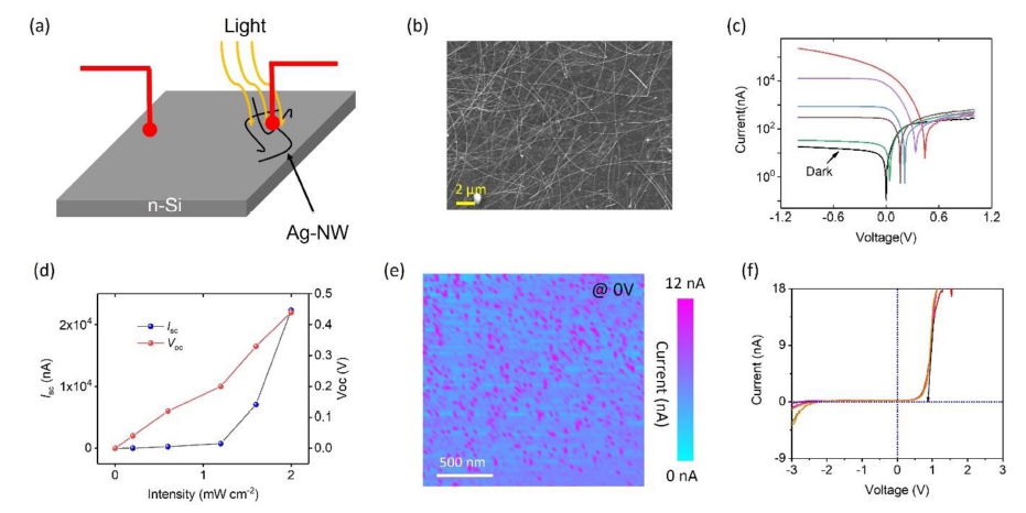
Fig. 1
(a) Schematic diagram of the AgNWs/n-Si Schottky junction. The light was illuminating over the AgNWs. (b) SEM image of the AgNWs, showing uniform distribution. (c) Current-voltage curves of the device under dark (black curve) and with continuous light (λ = 940 nm) illumination of different intensity. (d) The variation of the short circuit current (Isc) and open circuit voltage (Voc) as a function of illuminating intensity. (e) The current map from the Si with zero voltage tip bise, showing significant photocurrent. (f) Nanoscale IV curves collected from randomly chosen locations.
Initially, the measurements of current-voltage (I-V) curves were carried out under dark conditions, which verified the establishment of a Schottky junction [Fig. 1(c)]. In fact, the development of a barrier at the Si/AgNW interface was confirmed by the I-V characteristics, which were found to be nonlinear and asymmetrical [see black curve in Fig. 1(c)].9,20,21) Importantly, the formation of a junction-like structure, which can be properly characterized based on the band structures that are produced under conditions of zero bias, is thought to be the cause of the I-V characteristics that are observed in our device.18,22)
Indeed, the current on (I @ +1.0 V) and off (I @ 1.0 V) ratio is found to be higher than 17, indicating the formation of the junction. In addition, the variations in the I-V properties of the AgNW/Si junction were evaluated under illumination with a wavelength of λ = 940 nm, at different intensities ranging from 0.02 to 2 mW cm-2, in order to analyze the photoresponse of the device. Under the influence of the junction’s built-in potential, the fact that the photocurrent varies depending on the light intensity even when there is no external bias, which indicates that AgNWs/Si device can function as a self-powered photodetector. 16,23) Indeed, the I-V characteristics noticeably shift as a result of being exposed to light. For instance, an increase in the illuminating light intensity results in an increase in the current at 0 V. In point of fact, the photovoltage under light illumination rises in a linear fashion up to a maximum of 2 mW cm-2, as shown in Fig. 1(d). Light was illuminated on the top AgNWs to confirm that the build-in junction caused the charge carriers to separate, and a scanning conductive atomic force microscopy (AFM) probe was used to measure the current at a distance of 3 mm. The current map collected with zero tip bias (i.e., 0 V) is shown in Fig. 1(e). Clear current spots are noticed with zero bias, which indicates that the photogenerated charge carriers are separated by the junction. Further, the nanoscale I-V curves collected from randomly chosen points with scanning the voltage on the probe are shown in Fig. 1(f), showing the formation of the junction with a current on/off (Ion/Ioff) ratio of 18. Indeed, with the bulk and nanoscale measurements, it is clear that the AgNWs are forming a good quality Schottky junction, which is capable of separating the photogenerated charge carriers.
The photovoltaic effect takes place by the separation and collection of photogenerated electron-hole pairs by the electrodes. Therefore, it is to be anticipated that the photogenerated electron-hole pairs will flow all the way across the device even in the absence of an external electric field. As a preliminary test, the transient photoresponse (I-t) of the device was measured at λ = 940 nm with an intensity of 2 mW cm-2, as shown in Fig. 2(a). It is interesting to note that along with the study state photocurrent (i.e., direct photocurrent, Idc), a sharp peak during the light on condition appeared. This sharp peak is novel and cannot be explained by a simple photovoltaic effect; however, it is related to the quasi-Fermi level splitting and realignment. This effect is known as the ACPV effect, and the related current is depicted as Iac.16,19)
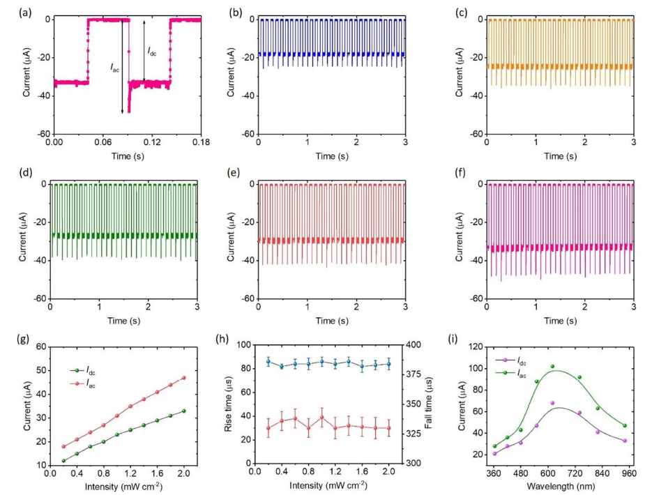
Fig. 2
(a) Transient photocurrent measured for a single pulse with zero voltage. The sharp peak indicates the Iac current whereas the constant current is related to direct current photocurrent (Idc). (b)-(f) Intensity-dependent photocurrent collected with 0 V. (g) The variation of Iac and Idc as a function of illuminating intensity for light (λ = 940 nm) intensity. (h) The rise and fall times as a function of light intensity. (i) The wavelength dependent Iac and Idc, showing broadband photosensing.
It is interesting to note that both Idc and Iac increase with increasing the illumination intensity of the light, as shown sequentially from Fig. 2(c) to 2(f). For clarity, the magnitude of the Idc and Iac with increasing light intensity is shown in Fig. 2(g). Note that both (Idc and Iac) increase linearly with intensity. This linear variation is critical for practical applications and ensures that both (Idc and Iac) are associated with photo-induced carrier generation and separation. For comparison, the photocurrent enhancement factor [i.e., ((Iac - Idc)/Idc) × 100 %] is found to 42 % for an intensity of 2 mW cm-2, which indicates that for the same illuminating intensity, the device is capable to generates a much higher Iac.
Further, the rise time (τr, i.e., time needed to increase the value from 10 to 90 %) and fall time (τf, i.e., time needed to decay from 90 to 10 %) is measured as a function of light intensity.4,23) The device shows an ultrafast response rise time of 36 μs, whereas the fall time was measured to 382 μs. It is interesting to note that the τr and τf did not show a significant change with intensity, which indicates that the generation of Idc and Iac is related to the junction only and that the role of interfacial defects is negligible.
Because the device is prepared with Si, and thus, broadband photosensing is expected. For confirmation, the Idc and Iac for different wavelengths starting from ultraviolet (UV) to near infrared (NIR) were measured and depicted in Fig. 2(i). Both Idc and Iac decrease close to the UV and NIR range, which matches well with the Si-based photodetector. This wavelength-dependent photocurrent dynamic indicates that the photocurrent is generated due to the absorbance in the Si. As a result of measuring the wavelength-dependent photocurrent production, the averages Iac and Idc can be shown in Fig. 2(i).
The responsivity (R) and detectivity (D) are out of these parameters to show the robustness of the photodetector. 24,25) Therefore, the photoinduced R and D values for dc and ac effects were calculated using the relation Rac/dc = Iac/dc/P, where P is the intensity, and where Id is the dark current, and the subscript corresponds to the ac or dc photocurrent. It is important to note that the magnitude of the Rac/dc and Dac/dc decreases gradually as the intensity increases, as shown in Fig. 3(a) and 3(b), respectively. The responsivity enhancement (E) via ACPV effect is calculated as, E = {(|Rac| − |Rdc|)/|Rdc|} × 100 %, increases with the incident photon density and reaches a maximum value of ~ 50 % at λ = 940 nm and 0.2 mW cm-2. It was found that the excellent performance was due to the strong electric field established at the AgNW/Si interface and the ACPV effect, which allowed the effective separation of photogenerated electron-hole pairs.
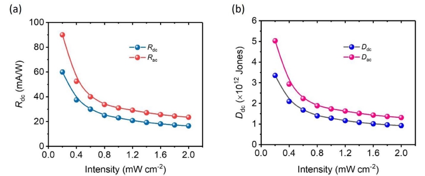
Fig. 3
(a) Responsivity corresponding to the direct current (Rdc) and ACPV effect (Rac) as a function of light intensity. (d) Detectivity corresponding to the direct current (Ddc) and ACPV effect (Dac) as a function of light intensity.
Examining the relevant research that has been published can provide a description of the functional mechanism underlying the ACPV effect. Under conditions of equilibrium, the Fermi levels of AgNWs and Si were in alignment with one another, and the concentrations of effective carriers did not change. Fig. 4(a) shows a representation of the band diagram at the AgNWs/Si interface under dark conditions, which reveals that this junction has the potential to serve as an optoelectronic device. A minimal variation in the electron density (Δe << e) is generated as a result of the fact that we are using n-Si. On the other hand, photo-produces e-h pairs in n-Si, which leads to an enhanced hole density.16,19) Therefore, a “slight” upward adjustment is made to the quasi-Fermi level (i.e. EFn) to reflect the change in electron density. On the other hand, a “substantial” shift in hole density is expected, which in turn leads to the quasi-Fermi level corresponding to holes (EFp) dropping, as shown in Fig. 4(b). Since the equilibrium condition is disrupted, and thus, a sharp peak in the photocurrent is also generated by light illumination, which causes the electron flow in the circuit until an equilibrium condition is reached [see Fig. 4(b)]. As can also be seen in Fig. 4(b), the amplitude of the built-in potential as well as the direction in which it points have an effect on the transfer of charge across the junction [see Fig. 4(c)]. In fact, the key behind the Iac generation is the splitting and realignment of the quasi-Fermi levels with an instant change in the illuminating conditions. This method shows that even a small change in the built-in potential can have a big effect on how the charge transfer works.
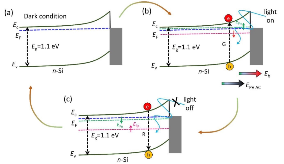
Fig. 4
Schematic diagram of the working mechanism. (a) Band alignment at the AgNWs/Si interface under dark conditions. Eg is the band gap of Si and, Ec, Ev, and Ef are the conduction band, valance band, and Fermi level, respectively. (b) Splitting of the quasi-Fermi levels with instant photo illumination. The G represent the generation of electron-hole pair. Eb is the junction built-in potential and EPVAC is the potential generated due to ACPV effect. Efn and Efp are the quasi-Fermi levels for the electrons and holes, respectively. (c) The recombination (R) of the e-h pair after removing the light.
4. Conclusion
In this work, we have demonstrated an ultrafast, selfpowered, broadband photosensor governed by the junction build-in potential and the ACPV effect. The photocurrent of the detector has been enhanced by 47 % due to the ACPV effect. The rise and fall times of the detector were measured at 36 and 382 μs. Further, the responsivity of the photodetector was enhanced by 50 % due to the AC PV effect. Overall, we demonstrated that with the effective utilization of the PCPV effect, the photosensing behavior of the AgNWs/Si Schottky junction can be enhanced. This study opens a new avenue to designing ultrafast and high performing photodetectors.
