

1. Introduction
In recent years, the demand for electronic circuits and antennas in mobile electronic devices, automotive and industrial applications has increased exponentially.1)
In addition, because the increase of the frequency band brings about the problem of noise in the electronic circuit, the demand for polymer composites having excellent processability, light weight, mechanical and electrical (dielectric constant) characteristics instead of metal materials has increased.
As a result, researches on the implementation of integrated circuits on polymer composite materials have been actively conducted.
These methods have technical limitations to achieve the presently required purpose, and new replacement processes are continuously being researched and developed for the purpose of commercialization.2-4)
One new methodology for producing metal tracks onto polymeric substrates is the so-called LDS (laser direct structuring) technology and is widely used for producing molded interconnect devices (MIDs).5)
LDS technology forms a conductive pattern by direct etching method using LPKF's specialized laser equipment.5) This method not only shortens the conductive pattern formation time, but also facilitates the formation of three-dimensional patterns, enabling direct use in the manufacturing field. LDS technology uses an injection molded product by adding an additive reactive with the laser to the thermoplastic resin. The surface of the injection-molded product is selectively processed with laser to form the desired pattern shape, and electroless plating is used to form the conductive circuit.
LDS technology uses organometallic additives that react with laser by which they are decomposed to act as a plating catalyst in the following electroless plating process.6-8)
Organometallic complexes based on palladium (Pd2+), copper (Cu2+)9) as well as metal oxide composites of copper−chromium oxide (CuO·Cr2O3) or antimony-doped tin oxide (ATO)10) have been used as catalyst sources for LDS technology in the last years.
However, since LDS technology uses special thermoplastic resin containing additives, it is difficult to realize thinning of circuits and various colors, and there are many restrictions on circuit design because of its weakness in strength.
Laser induced surface activation (LISA) is an advanced technology based on LDS technology. This method is not restricted by materials. General polymer resin can be used. As shown in Fig. 1, the integrated circuit implementation requires additional processing of the catalyst after the laser process, but the technological advantage is ample because it has flexibility in selecting the circuit substrate material.
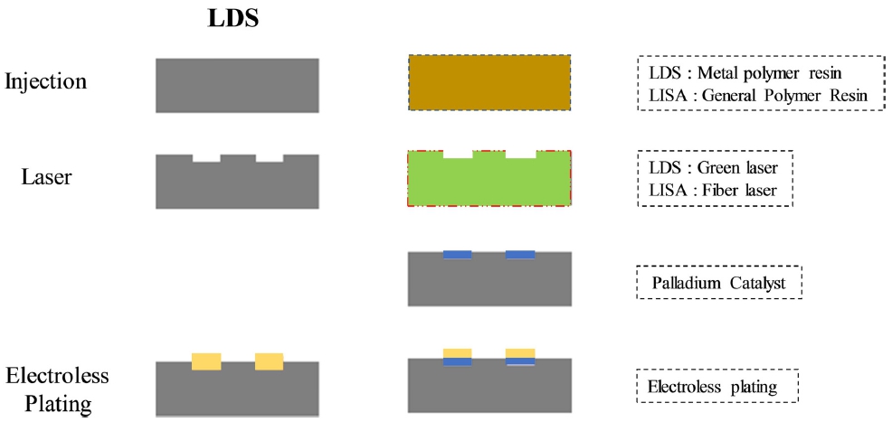
After the laser process, the catalytic process using a SnCl2/PdCl2 mixed solution on an insulator material is used.11)
There are some parameters which control the LISA process among which the laser process has the closest relationship with surface roughness of the circuit and as well as the adhesion of the circuit to the raw material and the accuracy of the circuit.
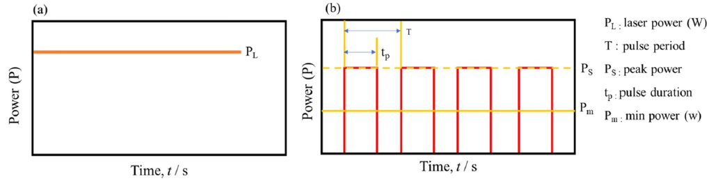
In this study, we investigate the effect of laser mode of continuous wave (CW) and pulse wave (PW) on the surface roughness and circuit accuracy in the Lisa process.
2. Experimental Methods
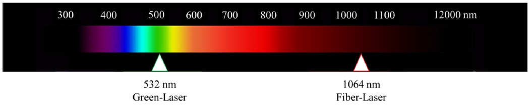
The polymer material used in the experiment was CF- 3200HF/GF 20 % (12 × 40 mm thickness, 3 mm) of Lotte Advanced Materials. As shown in Fig. 2, the laser equipment uses a (IPG, YLPM-20) fiber laser with a 1,064 nm wavelength in the near-infrared region. The laser condition is 15 watts of power, 20 kHZ of frequency, 100 mm of marking speed. Two laser conditions of CW type and PW type with waveform width of 100 ns were used as shown in Fig. 3.
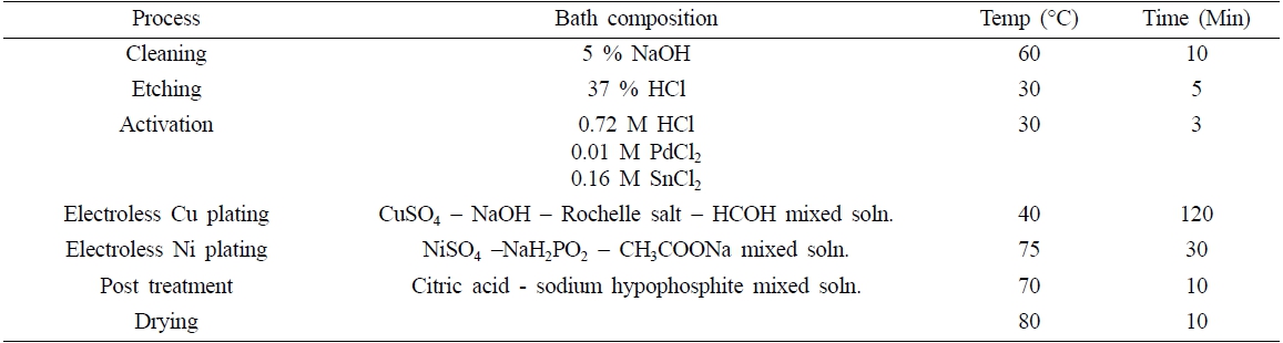
After the laser process, the sample was first immersed in a SnCl2 solution for 1-2 min at room temperature to adsorb Sn2+ ions on the surface. During the second immersion in a PdCl2 solution, Pd2+ ions are reduced by the Sn2+ ion through the reaction
The palladium metal clusters deposited on the substrate act as the active center to initiate the reduction of the metal in the subsequent electroless plating.12)
After the activation process, the circuit was subjected to electroless copper plating up to thickness of 10 μm and 3 μm electroless nickel plating using the process and chemicals as shown in Table 1.
The surface was observed using an optical microscope and the surface roughness was measured using a surface roughness tester (MITUTOYO, SJ-400). Measurements were made for an area of 0 .8 mm2 for each specimen. Ra represents the average surface roughness value from the measurement center line to the surface contour.
The cross-section and composition of the electroless conductive circuit-plated samples on the polymer material were observed using field emission scanning electron microscopy (FESEM). The specimens were cut, cooled, and polished with silicon carbide (SiC) paper, and the composition of the plating layer was analyzed using EDS.
3. Results and Discussion
Fig. 4 shows the digital microscopic images of the polymer material (a) and that after the laser irradiation in CW mode (b) and in PW mode (c). The figure also shows metal films formed by the electroless plating process after the both laser irradiations.
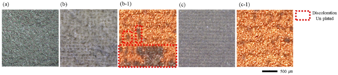
Fig. 4
Digital microscopic surface photographs of the polymer (a) before laser irradiation, and after irradiation in (b) CW mode and (c) PW mode. Surface photographs of the plated polymer after the laser treatment in (b-1) CW mode and (c-1) PW mode.
The surface roughness increased for all samples after the laser process by laser thermal energy.
CW laser treatment gave rise to traces of explosive craters and secretions on the surface, while PW laser treatment generated a relatively uniform surface.
After the plating process, the CW laser treated surface was covered with an uneven metal layer due to the rough surface formed in the laser process, while an uniform coating layer was formed on the PW laser treated surface.
Fig. 5 shows the surface roughness of the polymer material before and after the laser irradiation and the following plating process.
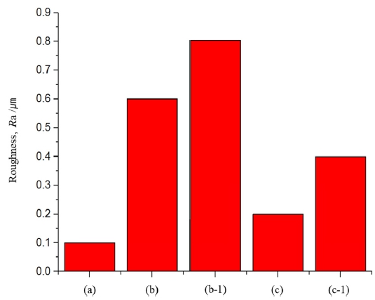
Fig. 5
Surface roughness of the polymer (a) before laser irradiation, and after irradiation in (b) CW mode and (c) PW mode. Surface roughness of the plating layer formed on laser treated polymer in (b-1) CW mode and (c-1) PW mode.
As the process progressed from laser treatment to plating, Ra changed from 0.6 to 0.2 μm for the CW laser treated samples and from 0.8 to 0.4 μm for the PW laser treated ones.
Fig. 6 shows FESEM images of the surface layer treated in CW and PW laser modes. In the CW laser mode, the surface was uneven, rough, and a small amount of burning occurred. The burning phenomenon is brought about by the thermal energy of the laser.
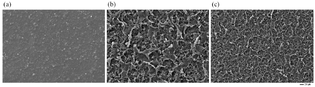
Fig. 6
Surface morphologies of the polymer (a) before, and after laser irradiation in (b) CW mode and (c) PW mode.
In the PW mode, the surface showed a relatively uniform shape and no burning occurred.
In both conditions, as the laser power increased, the size of the byproduct of the surface became larger, but the oxidized surface formed in the pulsed laser mode was relatively uniform in size of the byproducts and less defective.
Fig. 7 shows FESEM surface images of the electroless plated specimens after processing in CW and PW laser modes.
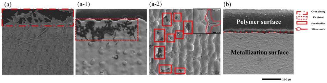
Fig. 7
Surface morphologies of edge of metallized surface formed on CW laser treated polymer (a, a-1, a-2) and on (b) PW laser treated one.
It was found that the surface of the specimen processed in the PW laser mode was superior to that in the CW laser mode in sharpness and linearity of the interface between the metallized and unmetallized polymer surfaces.
On the surface of the specimen treated in the CW laser mode, over-plating was observed at the interface between the metallized and unmetallized polymer surfaces. Un-plated spots due to the burning and discoloration phenomenon due to micro–cracks were also observed in the CW mode.
The discoloration phenomenon occurs because the plating solution is evaporated during the drying process at the microcrack portion where plating solution is absorbed.
The laser process improves the adhesion of the plating by forming fine irregularities on the surface to give a hooking effect.13)
Generally, a polymer is decomposed at a temperature higher than a certain temperature, and chemical bonds are broken. When a polymer composed of a combination of carbon, hydrogen and oxygen is decomposed by laser thermal energy, water (H2O), carbon dioxide (CO2) and carbon are generated.14)
Fig. 8 shows cross-sectional images of specimens to observe the surface activated layer formed under the conditions of each laser applied.
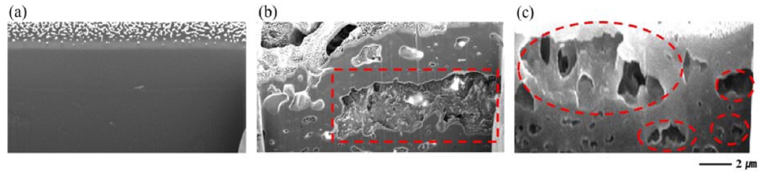
Fig. 8
Cross section of polymer (a) before and after laser irradiation in (b) CW mode and (c) PW mode.
In both CW and PW laser modes, pores due to laser thermal energy were generated.
However, in the CW laser mode, by-products due to the burning phenomenon existed on the surface of the polymer and pores of about 8 μm were formed inside the specimen.
These results are caused by the thermal energy generated by the CW laser, which causes the product to explode on the polymer surface, resulting in nonuniform and rough surface.
In the PW laser mode, there was no by-product from the burning phenomenon on the polymer surface. Pores of about 6 μm in width existed at the outer surface and these of 1 to 2 μm inside.
In the PW laser mode, even with same power as CW mode, the laser has an off-time of 100 ns, which works as a cooling time for the polymer surface. This allows the formation of relatively even surface roughness.
Therefore, in order to obtain a uniform surface, it is preferable to perform laser control in a PW mode rather than a CW mode.
These results are consistent with the observed trends in the surface morphology (see Fig. 4, 5).
Fig. 9 shows the cross-sectional structure after electroless copper plating and nickel-plating for specimens laser treated in CW mode (a) and PW mode (b). The nickel outer layer has a thickness of 2 to 3 μm and has an antioxidant effect. The thick intermediate layer determines the characteristics of the electric circuit with a thickness of 8 to 10 μm. The laser activated layer is very thin with a fine roughness that enhances the adhesion between the polymer material and the conductive metal layer.
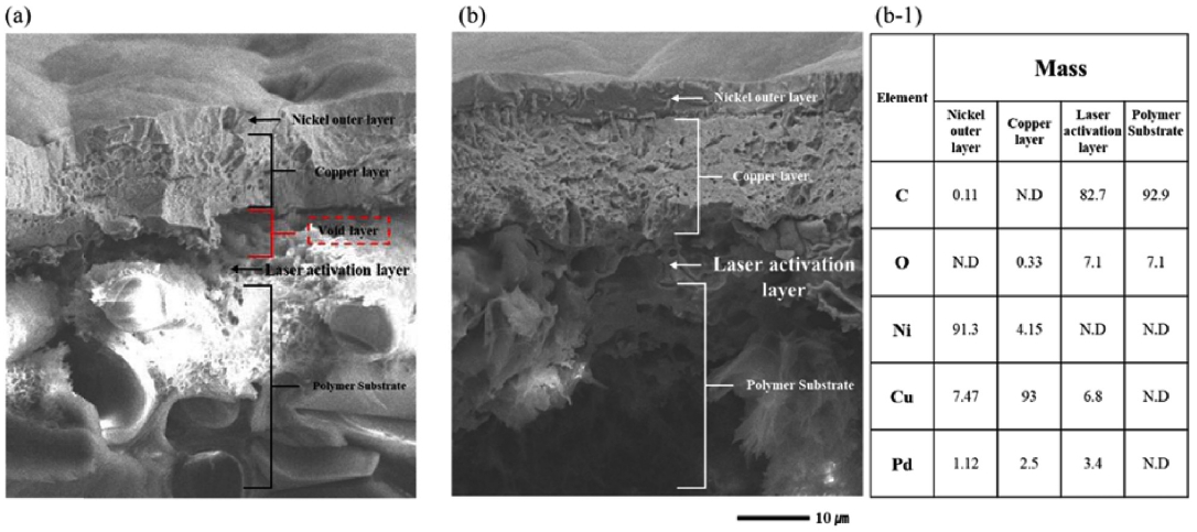
Fig. 9
Cross sectional structures of the plating formed on the polymer laser-treated in (a) CW mode and (b) PW mode. EDS analysis data are shown for the sample (b) in (b-1).
In the case of CW laser mode as shown in Fig. 9(a), there formed a void layer between the laser activated layer and the conductive metal layer after the plating process of the conductive metal. This results in a fatal defect in the bond strength between the polymer source material and the conductive metal circuit layer and can lead to local destruction of the conductive substrate. In contrast, no void layer was found in Fig. 9(b) for the specimen treated with a conductive metal plating process after the irradiation of pulsed laser. These results are consistent with the trend observed in cross-sectional and surface morphology (see Fig. 7, 8).
The EDS elemental analysis of the specimen (b-1) after the electroplating process for the specimen laser treated in PW mode showed that the polymer raw material was mainly composed of C and in the laser activated layer, O and Pd used as a catalyst were additionally distributed. In the electroless plated layer for the conductive metal circuit, Cu was the main component, and the outermost protective layer was mainly composed of Ni.
4. Conclusions
We demonstrate the applicability of the process to form conductive circuits using laser energy over polymer materials. The laser mode is evaluated to form a good conductive circuit, which can be optimized by obtaining an accurate and uniform circuit.
As the laser mode was changed from CW to PW mode, circuit surface defects were reduced. The surface roughness was also reduced. In the cross-sectional image, the pore size was relatively small and uniform. The conductive circuit consisted of the outermost nickel layer, the intermediate copper layer that determines the characteristics of the circuit, and the laser activated layer that determines the junction with the polymer material. Pd used as a catalyst in the laser activated layer was detected. Based on the results of this study, the use of pulsed lasers is advantageous for obtaining a more uniform and stable circuit when forming a conductive circuit on a polymer.
Sung-Hyung Lee
Gakkō hōjin Kitahara gakuen: Director
Shakai fukushi hōjin wayō-kai: Director
Iwate University yashiro ken research group: Special Researcher Hitoshi Yashiro
Iwate University: Professor Song-Zhu Kure-Chu
Nagoya Institute of Technology: Professor
