

1. Introduction
Germanium(Ge) has attracted significant attention as a channel material for the next generation nanoelectronics due to its high carrier mobility.1) One big obstacle for realizing high performance Ge n-channel metal-oxidesemiconductor field-effect transistors(MOSFETs) is the thermodynamically unstable germanium oxide(GeO) on the Ge substrate,2) which is easily desorbed from the GeO2/Ge substrate during the thermal process. The GeO volatilization to the air generates large amount of defects and traps at the GeO2/Ge interface.3,4) Numerous approaches such as nitridation, sulfur passivation, GeO2 passivation have been employed to passivate the Ge surface and thus, to improve the interfacial quality.5) Among them, GeO2 showed a promising result as a passivation layer with very low interface state density of ~1010 cm−2 eV−1.6) However, GeO2 has low conduction band offset of ~0.6 eV,7) which is very low to prevent the electron injection over the barrier and the direct tunneling through the GeO2 layer.8)
The high-k dielectrics can be used as an effective GeO2 capping layer that prevents GeO desorption from the GeO2/Ge interface.9) High quality of GeO2/Ge interface can be obtained when the inward diffusion of oxygen vacancy is suppressed,10) if not, can introduce defect states and degrade the device performance. According to the comparison of HfO2, LaGeOx, HfGeOy, GeNx, and Al2O3 as passivating gate dielectrics for Ge substrates, Li et al. also showed that a key role is to block oxygen vacancy diffusion through the GeO2.11) They suggested that Al2O3 is most proper material for this role, being a diffusion barrier and having large band offsets. Based on the calculation, it was demonstrated that AlN has fewer vacancy states in the Ge bandgap than Al2O3 and was suggested that AlN is a better choice for Ge MOSFET from the view of border trap properties, oxygen vacancy diffusion barrier, and band offset.12) Ge surface nitridation has also been found to successfully reduce the interface defect density,13,14) Therefore, AlN might passivate Ge or GeO2 surface better than Al2O3.
It was shown that combination of excellent thermal stability and large bandgap of Al2O3 and high dielectric constant of HfO2 produced better equivalent oxide thickness scalability with low interface state density on Ge than single HfO2 layer.15) In this respect, we employed a thin AlN as passivation layer on Ge and comparatively investigated the electrical properties of both HfO2/Al2O3 and Al2O3/HfO2 capping layers.
2. Experimental
Ga-doped, single side polished, Ge(100) wafers (thickness: 500 mm, resistivity: 0.01~0.1 ohm.cm) grown by Czochralski method were used in this work. The Ge wafer was first cut into small pieces and the samples were loaded into an thermal ALD chamber after cleaning process in a HCl:H2O (1:1) solution. The temperature was ramped up to 350 ºC to deposit 2.0 nm thick AlN layer using Trimethylaluminum(TMA) and NH3 as precursors. Then the temperature was lowered down to 250 ºC to deposit AlN protection layers with two different methods, (i) 1.0 nm thick Al2O3 was deposited first and then 2.0 nm thick HfO2 was deposited(denoted as HfO2/Al2O3) and (ii) 2.0 nm thick HfO2 was deposited first and then 1.3 nm thick Al2O3 was deposited(denoted as Al2O3/HfO2). Al2O3 and HfO2 films were grown by using the precursors of TMA and Tetrakis(ethylmethylamino)hafnium (TEMAHf), respectively, and H2O vapor was used as the oxidant. The thicknesses of the deposited films were measured using a FS-1 multi-wavelength ellipsometer. Metal-oxide semiconductor (MOS) capacitors were fabricated with an Al Schottky electrode(diameter: 500 mm, thickness: 50 nm) and a Pt back contact(thickness: 100 nm) in order to examine the electrical characteristics of the AlN/Ge interface. Capacitance–voltage(C–V) measurements were performed using a HP 4284A LCR meter and current– voltage(I–V) measurements were carried out with a Keithley 238 current source.
3. Results and Discussion
Fig. 1 shows the C–V curves measured at various frequencies. Below 100 kHz, the weak inversion humps are observed for two samples. The inset in Fig. 1(b) shows the normalized C–V data obtained from 500 kHz and 5 kHz. It is known that the hump area is proportional to the amount of mid-gap states.16) The C–V hump area was obtained by integrating the region bounded by two C–V curves measured at 500 kHz and 5 kHz. The C–V hump areas(i.e., Qhump) were estimated to be 3.41 × 10⁻⁷ and 5.41 × 10⁻⁷ C/cm2, respectively, for the Al2O3/HfO2 and HfO2/Al2O3 samples. This indicates that the HfO2/Al2O3 sample reduced the mid-gap states compared to the Al2O3/HfO2 sample. In addition, higher frequency dispersion in the inversion region was observed for the Al2O3/HfO2 sample. Strong dispersion in the inversion region observed for the nitrided Ge sample was associated with the presence of slow interface states,17) indicating the higher density of slow interface states for the Al2O3/HfO2 sample.
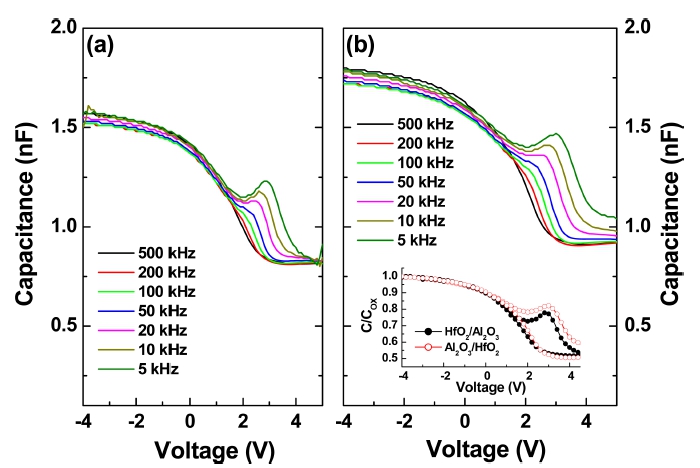
Fig. 1
Capacitance–voltage (C–V) data measured at various frequencies for the (a) HfO2/Al2O3 and (b) Al2O3/HfO2 samples. The inset in (b) shows the normalized capacitance values measured at 500 and 5 kHz.
Fig. 1 also shows that the accumulation capacitances are a little higher for the Al2O3/HfO2 sample as compared to the HfO2/Al2O3 sample. Al2O3 and HfO2 have large bandgaps(7.0 and 5.7 eV, respectively) and high dielectric constants(~9 and ~20, respectively).18) It was reported that the formation of Hf–Al–O by the intermixture of Al2O3 and HfO2 layers provided the dielectric constant between 9 and 20.19) The bonding energies of Al–O and Hf–O are known to be 501.9(± 10.6) and 801 (± 13) kJ/ mol, respectively.20) Hence, Al–O bonding would be dissolved more easily than Hf–O bonding. For the HfO2/ Al2O3 sample, the outdiffusion of Al atoms from the first-deposited Al2O3 layer might occur during the HfO2 deposition, leading to the formation of Hf–Al–O and decreasing the effective dielectric constant of dielectric layers. For the Al2O3/HfO2 sample, the outdiffusion of Hf atoms from the first-deposited HfO2 layer might not occur well during the Al2O3 deposition due to the higher bonding energy of Hf–O, suppressing the formation Hf– Al–O and producing the relatively higher effective dielectric constant of dielectric layers. Due to the difference in the effective dielectric constant, the different capacitance values were obtained. However, further investigation using x-ray photoelectron spectroscopy measurements is required in order to confirm this explanation.
Based on high–low frequency method, the interface state density(Dit) across the band gap was extracted using the following equation21)
where COX is the oxide capacitance at the accumulation, CHf and CLf are the capacitances at high and low frequencies. Here, COX values were obtained experimentally at 500 kHz from the accumulation region. In the calculation, 500 kHz and 1 kHz were selected as the high and low frequencies, respectively. Fig. 2 shows the Dit as a function of the gate voltage. Note that high-low frequency method can underestimate the Dit values because neither the 500 KHz nor the 1 kHz C–V data would be true high and low frequency curves, respectively. Nevertheless, this clearly shows that the HfO2/Al2O3 sample has lower interface state density than the Al2O3/HfO2 sample.
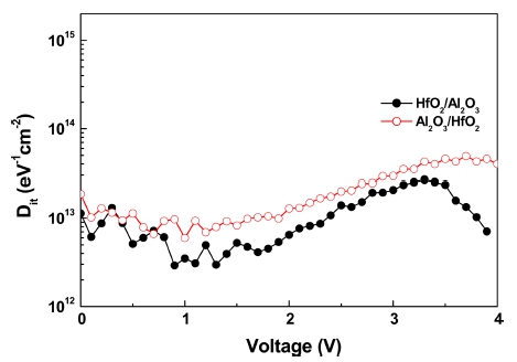
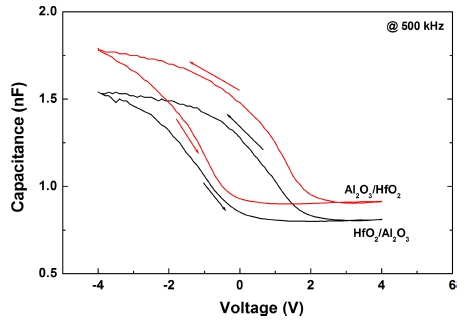
Fig. 3 shows the C–V hysteresis characteristics measured at 500 kHz. For both samples, a very large hysteresis was observed at the flat-band voltage(VFB), indicating the presence of high density of bulk oxide traps.22) The C–V hysteresis was also associated with the GeO volatilization,20) which could produce large amount of defects and traps in the high-k film.3) It is seen that the hysteresis C–V traces of both samples revealed the negative VFB shift, implying the positive charge trapping. Hole injection from p-type Ge substrate and trapping under the negative gate bias occurred higher than electron trapping under the positive gate bias during C–V hysteresis measurements.24) The average oxide trap densities (QT) along the Ge bandgap (Eg) were obtained through the relation QT = (COXΔVFB)/ qEg, where ΔVFB is the flatband voltage shift. The QT values were calculated to be 1.39 × 10¹³ and 1.86 × 1013 cm–2eV–1, respectively, for the Al2O3/HfO2 and HfO2/ Al2O3 samples.
Further investigation was performed by obtaining the parallel conductance values (Gp/ω) from the accumulation region.25)Gp/ω values as a function of radial frequency (ω = 2πf) were derived by Gp/ω = [ωGm(COX)2]/[(Gm)2 + ω2(COX − Cm)2], where Cm and Gm are the measured capacitance and conductance, respectively. These Gp/ω values can be connected with the following equation26)
where DT is the trap density and τT is the trap response time. The experimental and fitting data are shown in Fig. 4. The measured curves for the HfO2/Al2O3 and Al2O3/ HfO2 samples were resolved into one and two fitting curves, respectively. The energy level of traps above the Ge valence band, Et – EV were determined from τT according to the Shockley-Read-Hall statistics27)
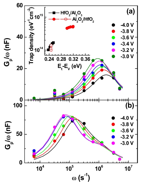
Fig. 4
Frequency dependent parallel conductance for the (a) HfO2/ Al2O3 and (b) Al2O3/HfO2 samples. The inset in (a) shows the obtained trap densities from the conductance method.
where vth is the thermal velocity, σp is the hole capture cross section (~1 × 10⁻¹⁶ cm2),28) and NV is the effective density of states in the Ge valence band. As shown in the inset in Fig. 4(a), the traps located at ~0.25 eV with the time constants between 0.5 and 1 μs were observed for both samples. These traps are likely to be located near the AlN/Ge interface. Meanwhile, the traps located at 0.3~0.32 eV observed for the Al2O3/HfO2 sample, which is not observed for the HfO2/Al2O3 sample. Because the time constants for these traps are 6~15 μs, they may be regarded as slow states. Border traps show a slower conductance response due to the time needed for the carriers to reach the traps within the AlN layer from the AlN/Ge interface. That is, these traps might be located within the AlN layer, which were generated during the HfO2 deposition.
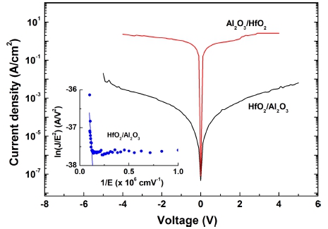
The leakage current density as a function of the voltage is shown in Fig. 5. At accumulation region, the gate leakage recorded the values of 3 × 10⁻³ and 2.3 A/cm–2 at -4.0 V for the HfO2/Al2O3 and Al2O3/HfO2 samples, respectively. This figure demonstrates a reduction of leakage current for the HfO2/Al2O3 sample by about three orders of magnitude, indicating again the better insulator quality. HfO2 is known to suffer from poor thermal stability and low crystallization temperature(500ºC), which produces large leakage current flowing along the grain boundary.29) Thermal stability experiments using the HfO2/Al2O3 bilayer in the AlGaN/GaN device have shown that improved device performance was due to the formation of the Hf–Al–O structure and the amorphous nature of the Al2O3 layer.30) Miyazaki et al. observed the larger leakage current using the HfO2 than that using the Al2O3 in the AlGaN/GaN device and they attributed this to the grain boundaries of the microcrystal in the HfO2 acting as the leakage path.31) The larger leakage current was also associated with a lower conduction band offset of 1.1 eV between HfO2 and GaN than that of 2.3 eV between Al2O3 and GaN.31,32) In addition, analysis of C– V characteristics of the HfO2/AlN stacks on GaN confirmed the dielectric constant of the HfO2 to be ~20, which is a typical value of ALD HfO2.33) This indicates that the outdiffusion of Al atoms from the AlN layer into the HfO2 layer was insignificant. As explained previously, the HfO2/Al2O3 sample might form the Hf–Al–O bonding more easily than the Al2O3/HfO2 sample. Based on these results, we can assume that the HfO2 layer in the Al2O3/ HfO2 sample did not underwent significant intermixing. Hence, the grain boundaries of the microcrystal in the HfO2 would not be affected in the Al2O3/HfO2 sample, which caused a larger leakage current. Consequently, Al2O3 is a better choice than HfO2 as the first deposition layer on AlN/p-Ge. As shown in the inset in Fig. 5, the forward bias current for the HfO2/Al2O3 sample was analyzed using the Fowler-Nordheim(FN) emission, given by J ∝ E2exp(−β/E).34) From the slope, the barrier height was calculated to be about 1.08 eV.
4. Conclusion
Using C–V and I–V measurements, we investigated the electrical and interfacial properties of HfO2/Al2O3 and Al2O3/HfO2 dielectrics on AlN/p-Ge interface. The inversion humps related to mid-gap states were observed for both samples, which was found to have lower mid-gap states for the HfO2/Al2O3 sample. High-low frequency method revealed the lower interface trap density for the HfO2/ Al2O3 sample. According to the parallel conductance method applied to the accumulation region, the border traps at 0.3 ~ 0.32 eV were observed for the Al2O3/HfO2 sample, which was not observed for the HfO2/Al2O3 sample. Therefore, it would be reasonable to assume that these traps were generated during the HfO2 deposition. The reduction of leakage current by about three orders of magnitude was observed for the HfO2/Al2O3 sample. These results clearly indicate the better insulator quality with an HfO2/Al2O3 dielectric stack.
