

1. Introduction
Recent developments in information technology and energy harvesting technology have prompted increasing demands for transparent conductive oxides (TCOs) as transparent electrodes forsuch devices as light emitting diodes, flat panel displays, smart glasses, and photovoltaic cells.1-3) Currently, tin-doped indium oxide (ITO) is widely used due to many desirable properties.3) However, shortage of the source material indium may raise price concern.4) In addition, technical problems such as poor mechanical flexibility5) and instability under hydrogen plasma ambient 6) may also restrict the application of ITO-based electrodes to some information or energy devices. One of the possible solutions to these problems would be to substitute ITO with ZnO made conductive by doping with B, Al, Ga, In, and F.2,4,7,8) To this date, Al-doped ZnO (AZO) and Ga-doped ZnO (GZO) have been most intensively studied using various deposition techniques.9) Despite many advantages, however, the ZnO-based TCOs are not free from drawbacks compared with ITO. Above all, ZnO films should be deposited at higher temperatures with larger thickness to achieve comparable sheet resistances to ITO counterparts, which may offset their advantages. If the ZnO-based TCOs are to be applied to the organic devices based on polymers, such a drawback would be a major obstacle to their applications. Therefore, it is necessary to establish process conditions that allow the deposition of the ZnOTCOs having reasonable properties at lowest temperature with smallest thickness possible.
A promising deposition technique serving this purpose seems to be the relatively recent technique of pulsed DC magnetrons sputtering (PDCMS). Incorporating the advantageous features of RF and DC systems,10,11) it allows high sputtering power in the range of few kW with high plasma density, long-term process stability with arc prevention, enhanced dynamic deposition rate enabling preparation of relatively defect-free films, etc.12-15) In the previous works, it has been demonstrated that the electrical properties of GZO films could be improved substantially at relatively low temperature and small thickness.16,17) In order to establish optimal thickness and deposition temperatures, however, it is necessary to understand how the changes in these parameters affect the microstructure of the films and resulting electrical properties. Unfortunately for ZnO, investigations so far indicate that there is no general correlation between the process parameters and the microstructures of the films, i.e., the correlation is dependent on the choice of deposition technique.18) Evenin the same category of deposition technique, the correlations may differ case by case.18) In the absence of any general model that predicts the grain structure of ZnO films as functions of process variables, it is necessary to understand systematically how the changes in the film thickness and deposition temperature are correlated to the film structure and electrical properties in the case of Ga-doped ZnO films deposited by PDCMS. In this study, effects of film thickness and deposition temperature are considered to explore the possibility of improving the electrical properties of the GZO films deposited by PDCMS at lower deposition temperature and at smaller film thickness.
2. Experimental Section
Ga-doped ZnO TCO films were deposited on glass substrates by pulsed DC magnetron sputtering (PDCMS). Glass substrates for typical liquid crystal displays (Corning Eagle 2000) were cleaned in trichloroethylene, acetone, and methanol in sequence and then rinsed in deionized water. On loading the substrate on the substrate holder located 160 mm away from the sputtering target, the sputtering chamber was evacuated to the base pressure of about 3.0 × 10⁻⁴ Pa. Subsequently, Ar (5N) gas was supplied into the chamber for the film deposition at the working pressure of 0.67 Pa. Before the film deposition, presputtering was carried out for 10 min. to remove any contaminants on the target. A square-shape ZnO ceramic targets (400 mm × 400 mm) containing 5.7 wt% of Ga2O3 were used as the sources. Sputtering power was fixed at 2.4 kW with the pulse frequency of 50 kHz and the duty cycle of 72 %, which gave the pulse factor of 14.4 μs. Deposition temperatures were varied between room temperature (RT) and 250 °C. Deposition thickness of the GZO films were varied between 50 and 500 nm by controlling the deposition time based on the calibrated deposition rates. Electrical propertieswere measured by a van der Pauw Hall method (Bridge Technology, Ecopia HMS-3000 Hall Measurement System) at room temperature with the applied magnetic field of 0.55 T in a dark condition. Optical transmittance was measured using a UV-VIS spectrometer (JASCO, V-570) in the wavelength range of 200-800 nm. Crystallinity of the films was analyzed by x-ray diffraction (XRD) in θ-2θ scan mode using a Ni-filtered CuKα1 source (Philips X’pert MPD 3040). Microstructural evolutionof the films with varying temperature and thickness was investigated using a transmission electron microscope (TEM, JEOL JEM-3010).
3. Results and Discussion
Fig. 1 shows how the electrical properties of the GZO films change with varying deposition temperatures, T, for various film thicknesses. In Fig. 1(a), the electrical resistivity changes with two opposed trends with varying thickness, depending on the deposition temperature. For T = 25 to 150 °C, the resistivity decreases rapidly as the thickness increases from 50 to 200 nm initially and then remains almost constant with further increasing the thickness (trend 1). While the lowest resistivity of 3.33 × 10⁻⁴ Ωcm was achieved when the GZO film was deposited at 150 °C to the thickness of 300 nm, the 200 nm sample shows the comparable resistance of 3.73 × 10⁻⁴ Ωcm. Contrary to this, for T = 250 °C, the resistivity increased continuously with increasing thickness (trend 2). In this case, the lowest resistivity of 5.49 × 10⁻⁴ Ωcm was obtained at the film thickness of 50 nm. For the film deposited at 200 °C, the resistivity initially decreased to 5.50 × 10⁻⁴ Ωcm as the thickness increases to 100 nm, but it increased slightly and monotonically with further increasing the thickness.
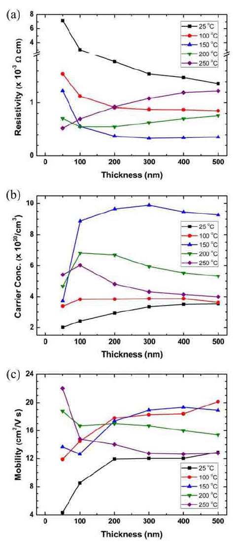
Fig. 1
Changes in the electrical properties of the GZO films deposited at various temperatures plotted as functions of the film thickness: (a) electrical resistivities, (b) Hall mobilities, and (c) carrier concentrations.
The changes in the carrier concentration and carrier mobility are shown in Figs. 1(b) and 1(c), respectively. For the films deposited at 25 and 100 °C, the carrier concentration increases only slightly (25 °C) or stay almost unchanged (100 °C) with increasing thickness whereas the Hall mobility increases rapidly with increasing thickness to 200 nm and then slightly with further increasing the thickness. On the other hand, films deposited at 200 and 250 °C show decreasing carrier concentrations with increasing thickness after the initial increase at the thickness of 100 nm. Meanwhile the Hall mobilities decrease continuously with increasing thickness after relatively large decrease at the thickness of 100 nm. For the GZO film deposited at 150 °C, substantial increase in the carrier concentration with increasing thickness to 100 nm is followed by a small increase to the maximum at 300 nm and then slight decrease subsequently. The Hall mobility of these films in general increases with increasing thickness after initial crease at 100 nm. It is noticed in Fig. 1 that the carrier concentration and Hall mobility are dependent not only on the deposition temperature but on the film thickness especially in the small thickness regime. Since the film thickness was controlled by varying the deposition time, it is deduced that the increase in the films thickness is related to the time-dependent microstructural evolutions which assist the activation of donor Ga and improvement of crystalline quality, affecting the electrical resistivities in two opposed trends.
Fig. 2 shows the representative XRD patterns that exhibit microstructural developments of the GZO films in relation to the changes in the film thickness and the deposition temperature. The strong diffraction peaks at 2θ = ~34.4° commonly observed in all the films are due to (002) planes of wurtziteZnO (JCPDS 36-1451). This indicates that all the films have hexagonal lattices oriented along the c-axis normal to the substrate. Diffraction peaks related to ZnGa2O4 and Ga2O3, which can be formed when Ga concentration is high, are not traced in the XRD patterns. In Fig. 2, for the deposition temperatures of 100 °C, the diffraction intensities of the ZnO (002) peaks increase continually in height with increasing film thickness. On the other hand, for the deposition temperatures of 150 and 200 °C, the intensities of the (002) peaks increase only slightly with the film thickness up to 200 nm and then remain almost constant with further increasing the thickness, which is accompanied by the appearance of ZnO (101) peaks at 2θ = ~36.2° (JCPDS 36-1451). Meanwhile, when the XRD spectra for the films having the same thickness are compared (300 nm for instance), the height of ZnO (002) peak decreases with increasing deposition temperature, which is accompanied by peak broadening with the appearance of the (101) peaks.
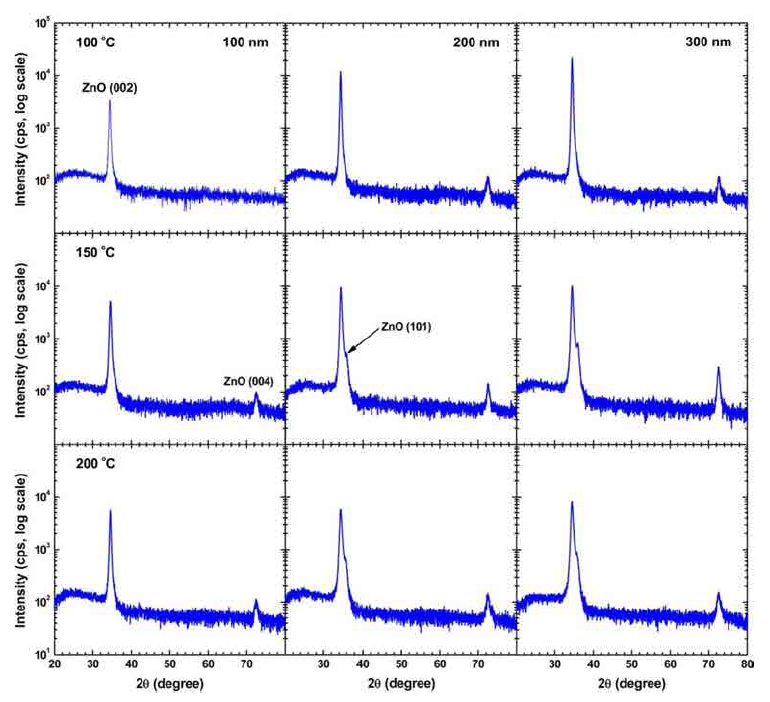
Fig. 2
Microstructural evolutions of the GZO films with varying deposition temperature and thickness as revealed in the XRD patterns.
Observations in XRD patterns are supplemented by the TEM. Fig. 3(a) shows the high resolution (HR) fringe patterns of the GZO films deposited at 150 °C. In these HR images, the designations of ‘bottom’, ‘middle’, and ‘top’ refers to the region close to the substrate/film interface, the mid-layer region, and the region close to the top surface, respectively. In Fig. 3(a), the fringe patterns representing the (002) plane are dominantly parallel to the film/substrate interface (the direction normal to these planes is denoted as ‘main orientation’) in the bottom region indicating that the grain growth followed the preferential nucleation.18) On the other hand, some of the (002) planes have different orientations in the top regions when the thicknesses are 200 and 500 nm (these orientations are denoted as ‘orientation 2’). In addition, the degree of misorientation (angle between the main orientation and the orientation 2) is much larger in the 500-nm-thick film. In the accompanying selected area electros diffraction (SAED) patterns taken from the top regions (Fig. 3(b)), it is seen that the diffraction spots are more randomly arranged with increasing film thickness, revealing the increasing structural disordering with increasing thickness.Fig. 4
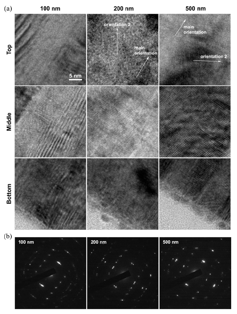
Fig. 3
(a) HRTEM fringe patterns showing the textural evolution of the GZO films deposited at 150 °C and (b) accompanying SAED patterns obtained for the top regions of the films.
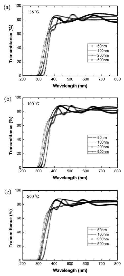
Fig. 4
Optical transmittance curves or the GZO films deposited with various combinations of deposition temperature and thickness.
There is no general or universal model that describes the microstructural development of ZnO films. However, the above XRD and TEM observation supports the assertion suggested by Lee et al.19) It has been reported that structural evolution from the c-axis preferred orientation to the mixed orientation is promoted by the bombardment of energetic oxygen ions even under pure Ar atmosphere during magnetron.19) Concerning the origin of oxygen, it is believed that oxygen ions were generated within the plasma since the sputtering target contains high fraction of oxygen as a component element (both in ZnO and Ga2O3). Especially, substitution of lattice Zn ions by Ga ions would occur on the premise that Ga2O3 is chemically decomposed during the sputtering. When the surface of growing ZnO film is bombarded by energetic oxygen ions, crystal growth tends to occur in the way to minimize energy loss per unit area caused by the surface damage. Such energy loss minimization can be achieved by the growth of (10l) planes in preference to the (002) plane since the former have lower packing density. Growth of (10l) planes is further promoted if the deposition temperature is higher and films become thicker. In one extreme, it is even possible that the ZnO films have the a-axis orientation19) (a-axis in this sense include the [100], [101], and [110] direction18)). The observations on the crystallinity by XRD in this study are consistent with these explanations. In this regard, it is suggested that the energy loss minimization model can describe the microstructural develop- ment process in the ZnO films deposited by PDCMS.
Regarding the optical properties of the GZO films, their transmittance in the visible spectrum (400 to 700 nm wavelength) did not show strong dependence on the thickness and deposition temperature as seen in Fig. 5. The films having the thickness of 100 nm and higher have the transmittance of about 80 % for the 550 nm wave, which satisfies the requirement for the transparent electrode. In comparison, transmittance of the 50-nm-thick films was somewhat lower than 80 %. If it is assumed that the micro-structural evolution is a time-dependent process, since the thickness was controlled by adjusting the deposition time, it is expected that the 50-nm-thick films do not have well-developed microstructure especially when lower deposition temperature was applied.
The experimental observations so far suggest that the deposition of GZO films at moderate temperature with relatively small thickness is desired to achieve good electrical properties when the GZO films are deposited by PDCMS. Such process condition would also beneficial for process simplification and cost saving. For instance, the sheet resistance of the 200-nm-thick film deposited at 150 °C is 18.2 Ωsq-1. Applicability of such an ‘optimal’ or ‘near-optimal’ condition was verified by depositing the GZO films on a transparent polymer substrate of polyethylene naphthalate (Teonex® PEN, product of DuPont) which is one of the candidates for flexible electronics and has the glass transition temperature of 120 °C. Table 1 summarizes the electrical properties of the GZO films on the PEN substrate deposited at 25 °C and 100 °C with the thickness of 50 and 100 nm, respectively. Except for the film deposited at 25 °C with the thickness of 50 nm, all the films have the carrier concentrations in the low 1020 cm-3 range and the mobility well exceeding 10 cm2V-1s-1, which yield the resistivity in the low 10-3 Ωcm range. While there is a room for improvements, reasonable electrical property has been achieved in that the lowest sheet resistance estimated from the resistivity and thickness in Table 1 would be 210 Ωsq-1.
4. Conclusions
When Ga-doped ZnO films are deposited on glass substrates by pulsed DC magnetron sputtering, preferred nucleation allows initial c-axis orientation of the ZnO grains. However, bombardment of energetic species promotes the structural disordering which leads to the appearance of a-axis oriented grains. Consequently, improvement of crystalline quality of individual grains with increasing deposition temperature and time (thickness) is offset by the disordering of the overall textured structure of the GZO film typified by columnar grains. Such a micro-structural evolution process results in the achievement of ‘optimal’ electrical properties of the GZO films at relatively low deposition temperature at small thickness since higher temperature and larger thickness are instead detrimental to the improvement of the electrical properties. In the case of the current study, sheet resistance comparable to that of the commercially available ITO electrode could be obtained at the deposition temperature of 150 °C with the thickness of 200 nm. At even lower temperature and smaller thickness, reasonable electrical property could be obtained which enabled the deposition of GZO TCOs on the PEN substrates demonstrating the applicability of the low-temperature deposition technique to the polymer-based flexible electronics.
