


1. Introduction
A dye-sensitized solar cell(DSSC), as one of the thirdgeneration solar cells, has benefits including the low cost, the applicability on flexible substrates, and the capability for large-scale production than silicon-based solar cells that are most widely used today. Thus, it has high potential for commercialization in the future.1-3) However, the energy conversion efficiency(ECE) of DSSC has only reached around 11 % and many researches are currently ongoing to improve the photoelectric efficiency.4)
In order to improve the ECE of a DSSC, components such as dye, electrolyte, and working electrode(WE) have been actively investigated.5) So far, the research on WE has been reported to be the most effective.
A WE of a DSSC is consisted of fluorine-doped tin oxide(FTO) electrode, blocking layer(BL), TiO2 layer, and dye, and investigations on improved performance of TiO2 layer are highly popular.6-7) TiO2 layer largely functions as an electron movement path that transports electron formed at dye to the electrode and as a porous structure providing a space for dye absorption. Studies to enhance each function are taking place as followings.
First, the band gap can be tuned to improve the performance of TiO2 layer as an electron movement path. S. Lee et al.8) injected Nd in the TiO2 layer to change the band gap, and reported that the increase in ECE from 6.6 % to 7.3 %. Y. Yao et al.9) employed carbon nano tube into the TiO2 layer to yield a narrower band gap than that of pure TiO2 layer and obtained an improved ECE.
Secondly, techniques such as making a thicker TiO2 layer and coating TiO2 in multi-layers to provide an additional space for dye adsorption exist to modify the mesoporous structure for enhanced dye absorption.10) However, the diffusion length of the electron at dye is limited to approximately 12 μm.11) If TiO2 layer is formed to have a greater than proper thickness, the electron fails to reach the electrode and gets lost, resulting in lower ECE. Therefore, it is desirable to increase dye absorption without charge recombination at the optimum layer thickness of TiO2. Recently, researchers are exploring ways to engineer shape and micro structure of TiO2 particles. H. Xu et al.12) reported an increased surface area and ECE by employing nano tube-shaped TiO2 particles instead of sphere TiO2. S. Agarwala et al.13) controlled the size of TiO2 particles to decrease the porosity size. The surface area increased, and thus dye absorption improved. Also, a study employing PVC-g-PNVCL, which can be selectively decomposed, was done to form highly porous TiO2 layer and improve dye adsorption.14)
Polymethyl methacrylate(PMMA), one of plastic materials, is made by polymerization of methyl methacrylate (MMA) monomer and has characteristics of clarity and coloring ability. It is widely used as various parts and construction materials. Also, molecular chains are easily broken at the 300~400 °C and are decomposed to MMA monomers. Because decomposed monomers are volatile, PMMA, along with poly styrene, is used as a poreforming agent to form nano-sized pores.15-16) If PMMA is employed into the TiO2 layer of the WE in DSSC, nano scale porosity can be formed in the TiO2 layer by annealing process at 500 °C. The surface area will increase, and consequently, improved ECE of DSSC is expected. In this study, we made nano-scale PMMA and added 0.0~1.0 wt% PMMA into the TiO2 layer in DSSC to confirm an improved ECE.
2. Experimental Procedure
The BL of WE was made by mixing titanium(IV)bis (ethyl aceto acetato)-diisopropoxide and 1-butanol into a solution, followed by spin-coating at conditions of 500 rpm-10 sec and 2000 rpm-40 sec and heat treatment at 500 °C for 15 min.
To observe the changes in photoelectric properties of DSSCs in response to PMMA addition, we fabricated the semiconducting TiO2 layer by dispersing PMMA of 0.0~1.0 wt% into the TiO2 paste(20 nm, DSL 18NR-T of 10, Dyesol) with a glass rod for 30 minutes.
Nano-scale PMMA was synthesized with MMA monomers. 0.81 M of MMA was added into a sealed glass with 10.9 mM of ammonium persulfate, 50 mL of acetone, and 50 mL of deionized water. Mixed solution was stirred at 75 °C for 3 hrs. Synthesized PMMA dispersion was dried at 65 °C for 2 days in a dry oven. To analyze the microstructure of synthesized PMMA, transmission electron microscopy(TEM, HF-3300, Hitachi) was used. PMMA was dispersed in ethanol by using ultrasonic agitator to prepare the sample.
To coat the semiconducting TiO2 layer on top of the previously fabricated BL, TiO2 film was formed by coating the TiO2 paste with 0.0~1.0 wt% PMMA via doctor blade method and by treating under heat at 500 °C for 30 min. Then, we obtained the glass/BL/TiO2+ PMMA structure.
We analyzed the surface and cross-sectional microstructure of the TiO2 layer with PMMA by using field emission scanning electron microscope(FE-SEM, S-4800, Hitachi) at an accelerating voltage of 15 kV.
Also, to check for an increase in specific areas of TiO2 layer as a result of PMMA addition, an area of 4 × 4 μm2 was scanned in non-contact mode by using an atomic force microscope(AFM, SPM25DRM, Park Scientific Instruments) and surface roughnesses were checked by measuring root mean square(RMS). Here, the samples were prepared by coating the TiO2 film with 0.0~1.0 wt% of PMMA on a flat glass substrate.
We adsorbed 0.5 mM cis-vis bis-ruthenium(II) bistetrabutylammonium( N719) on a TiO2 and completed the WE consisted of glass/FTO/BL/TiO2+PMMA/dye(N719).
Absorbance of the prepared WE was analyzed by UVVIS- NIR(UV3105PC, Shimadzu) with an absorption-mode apparatus under medium scan speed. Average absorbance in the visible-light region of 400~800 nm was obtained by adding absorbances at each wavelength and dividing it by the number of added times.
The counter electrode(CE) was prepared by RF sputter (MHS-1500, Moohan, 300 W, 13.56 MHz) to form a 100 nm-Pt film on a glass substrate using 99.99 % Pt as a target. A flow of 40 sccm Ar at pressure of 5 mtorr at room temperature was used for the process.
The prepared WE and CE were combined at position and were filled with electrolyte, finalizing DSSC device consisted of glass/FTO/BL/TiO2+ PMMA/dye(N719)/electrolyte /100 nm Pt/glass with active area of 0.45 cm2.
Impedance of DSSC was determined by solar simulator (PEC-L11, Peccell) and potentiostat(Iviumstat, Ivium) to verify interfacial resistance. The analysis was carried out in the frequency range of 10 mHz ~ 1 MHz applying AC voltage and the current responses were collected. The Nyquist plot for the impedance was determined to be the resistance from charge transfer at the Rs and TCO/TiO2 (Rh), charge transfer at the electrolyte/CE and TCO/TiO2 (R1), charge transfer at the TiO2/electrolyte and electron mobility(R2), and the Warburg impedance for redox diffusion in an electrolyte(R3).
I-V(current-voltage) characteristic of DSSC was measured by the same instruments under a setup using a 100 W Xenon lamp as the illumination source at 1 sun(100 mW/cm2) condition. From the I-V curves, short-circuit current density(Jsc), open-circuit voltage(Voc), fill factor (FF), and ECE were determined.
3. Result and Discussion
Fig. 1 is a TEM image of synthesized nano size PMMA observed at 25,000 times magnification. The result of TEM analysis shows that PMMA particles have sphere form with the average size being approximately 80 nm. Therefore, we confirmed that PMMA was successfully synthesized in nano-scale. However, we observed agglomeration of nano-particles and the average size of agglomeration was 300 nm. When constructing a PMMAemployed TiO2 layer, the size of formed agglomerate can be larger compared to that of individual PMMA particles.
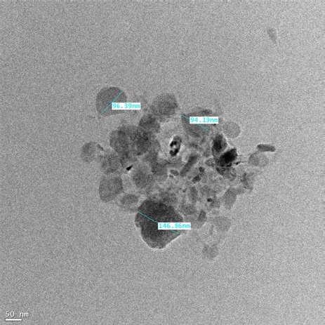
Fig. 2 shows FESEM images of the TiO2 layer with 0.0, and 1.0 wt% of PMMA at 20,000 magnifications. Insets at the upper-right corner are images of crosssectional image of 5,000 magnifications.
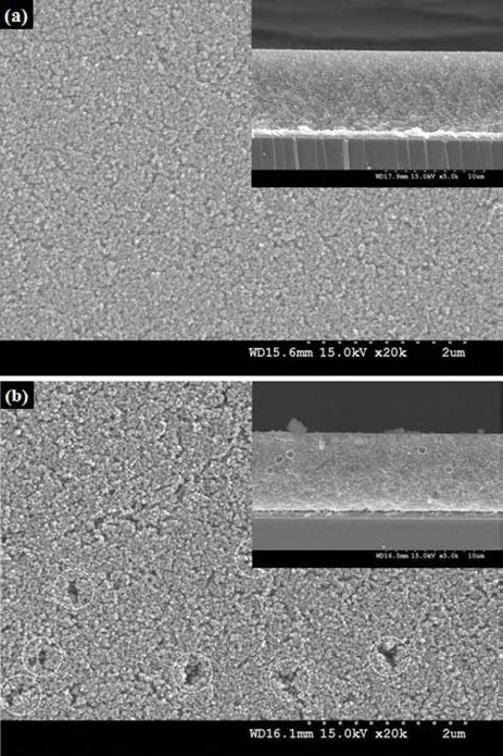
Fig. 2
FESEM images of surface section of TiO2 layers with PMMA of : (a) 0.0 wt%, and (b) 1.0 wt%. Insets are cross-sectional FESEM images of TiO2 layers.
According to Fig. 2(a), which is the surface image of TiO2 layer without PMMA, TiO2 layer was coated relatively uniformly without any macro-size pore and was composed by 20 nm TiO2 particles. Meanwhile, inset at the upper-right corner shows the cross-sectional image of Fig. 2(a), indicating that the TiO2 layer is 8 μm thick and is structurally uniform without any pore-like surface image. Fig. 2(b) shows the surface image of TiO2 layer with 1.0 wt% PMMA. As with Fig. 2(a), it is consisted of 20 nm TiO2 particles, but sphere pores with the density of 0.28 ea/μm2 were formed as indicated by the white dotted-line. Considering that the thermal decomposition temperature of PMMA is about 300 °C, sphere pores are formed after sintering at 500 °C by thermal decomposition of added PMMA. Also, the average size of pores is about 200 nm and the average size of PMMA agglomerate is about 300 nm as shown in the TEM result of Fig. 1. Based on these observations, pores shown in FESEM image must have been formed by the thermal deposition of PMMA agglomerates. Meanwhile, inset at the upper-right corner shows that the TiO2 layer was deposited to have about 8 μm thickness. As in the surface image, the pores are formed by thermal decomposition of PMMA in the part marked with dotted-line. Therefore, we confirmed that the nanoscale pores can be successfully formed in the TiO2 layer by adding PMMA of 0.0~1.0 wt%.
Fig. 3 shows the rms values of PMMA-added TiO2 layer measured with AFM. When PMMA is added up to 1.0 wt%, the average rms values of TiO2 layer were measured to be 25.2 nm, 27.4 nm, 28.7 nm, 30.8 nm, 32.3 nm and 34.8 nm. This observation concurs with the previous FESEM analysis result in that the linear increase in the surface roughness is caused by the increase in the surface area, which is due to the pore formation after the PMMA thermal decomposition. As a result, we indirectly confirmed that the surface area of TiO2 layer can be increased effectively by employing PMMA, which is a thermoplastic polymer.
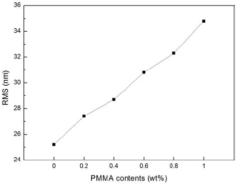
Fig. 4 shows absorbance curves of the WE with PMMA at the visible-light range of 400~800 nm. The average absorbance of WE without PMMA is 0.177 %, while they are 0.191 %, 0.191 %, 0.191 %, 0.198 %, and 0.209 % with the addition of PMMA of 0.2, 0.4, 0.6, 0.8, 1.0 wt% of PMMA respectively. This increase of absorbance with the addition of PMMA is attributed to the increased dye adsorption on the porous TiO2 layer, which results from the increased surface area after the pore formation. The increase in specific surface area of the TiO2 layer with PMMA agrees with microstructure and rms result discussed before. Therefore, dye absorbance can be enhanced by adding PMMA and forming pores.
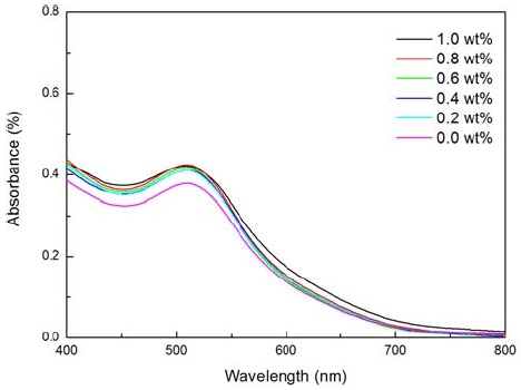
Fig. 5 is the nyquist plot consisted of real and imaginary terms for DSSC structured as glass/FTO/blocking layer/ TiO2+PMMA/dye(N719)/electrolyte/100 nm Pt/glass with PMMA under applied frequency. It is evident that the curves show three half-circles(R1, R2, R3) like an internal resistance curve of conventional DSSC.
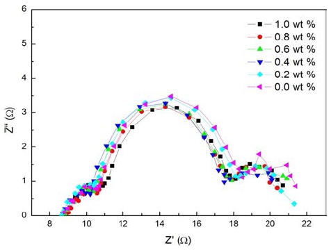
R1 value represents interfacial resistance at the CE/ electrolyte in the frequency region of 103-105 Hz, and it is about 1.3 Ω for all cases since the CE and electrolyte are the same for all DSSCs.
In the case of R2 value, which represents electron transport resistance of TiO2 layer in the frequency region of 1-103 Hz, it was 7.9 Ω without PMMA. However, adding PMMA of 0.2, 0.4, 0.6, 0.8, and 1.0 wt% yielded R2 values of 7.9, 7.5, 7.3, 7.3, and 7.1 Ω respectively, showing a decreasing trend. This is attributed to PMMA addition that makes the TiO2 layer porous, which yields increased specific surface area for dye absorption.
R3 value at a frequency higher than 106 Hz is related to diffusing redox species within the electrolyte. R3 values are all about 2.8 Ω, since the electrolyte is the same.
Thus, we confirmed that the addition of PMMA increased dye adsorption for electron generation and that the increased electrons ultimately reduce resistance.
Fig. 6 is I-V data of DSSC with PMMA. We confirm that adding PMMA results in a higher Jsc compared to the case without PMMA, and this result is related to the electron generation. PMMA added device has higher Jsc than the one without PMMA. As with the change in R2 value of impedance, this observation can be explained by increased dye absorption with the addition of PMMA and thus increased electron generation. Also for the FF, which is related to the surface resistance of DSSC device as a whole, the FF of PMMA added device was observed to be greater than the device without PMMA.
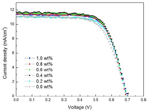
Table 1 shows the values used for I-V curves of Fig. 6. Voc depends on both redox level of electrolyte and fermi level of TiO2 electrode. Since we used the same electrolyte and TiO2 electrode, the Voc was measured to have the same values within the margin of error regardless of the amount of PMMA addition.
Table 1.
Photovoltaic properties and energy conversion efficiency of DSSCs with PMMA of 0.0~1.0 wt%.
| PMMA contents (wt%) | Voc(V) | FF | Jsc(mA/cm2) | ECE(%) |
|---|---|---|---|---|
| 0.0 | 0.69 | 0.638 | 11.16 | 4.91 |
| 0.2 | 0.69 | 0.656 | 11.14 | 5.06 |
| 0.4 | 0.69 | 0.654 | 11.73 | 5.35 |
| 0.6 | 0.69 | 0.657 | 11.68 | 5.31 |
| 0.8 | 0.69 | 0.661 | 11.54 | 5.24 |
| 1.0 | 0.70 | 0.654 | 11.45 | 5.22 |
FF with PMMA of 0.0, 0.2, 0.4, 0.6, 0.8, 1.0 wt% was 0.638, 0.656, 0.659, 0.657, 0.661, 0.654, respectively. It indicates a clear increasing trend as the amount of added PMMA increases.
Jsc of the device with 0.4 wt% PMMA was 11.73 mA/ cm2. Compared to that of the device without PMMA, which was 11.16 mA/cm2, it showed the improvement of approximately 5 %. This can be explained by the increased electron generation. During the thermal process for sintering of PMMA added TiO2 layer, PMMA thermally decomposes and form pores. The pores enhances dye absorption, which results in more generation of electrons. Later when the amount of PMMA addition was greater than 0.6 wt%, the Jsc rather decreased. It was considered to be the result of a relative reduction in the fraction of TiO2 layer as an electron transport material as the amount of pores increased.
The final ECE of the DSSC without PMMA was 4.91 %, while the efficiency of device with 0.4 wt% PMMA was 5.35 %. However excessive PMMA more than 0.6 wt% ECE was decreased, this result depend on Jsc change. Yet, adding more than 0.6 wt% of PMMA resulted in decreased ECE, which coincides with the change in Jsc.
Therefore, we successfully fabricated DSSC devices of enhanced ECE by adding proper amount of PMMA into the TiO2 layer to increase specific surface area.
4. Conclusion
We observed the change in properties of a DSSC with WEs employing nano-sized PMMA beads. We successfully manufactured PMMA beads of 80 nm and employed 0.0~1.0 wt% PMMA on TiO2 layer. Microstructure analysis confirmed the increase in surface area when PMMA is added to form porous TiO2. According to the absorption analysis, the degree of absorption increased as the amount of PMMA added increased. The final ECE of the manufactured DSSC was 5.35 %, which was 8 % improvement compared to the one without PMMA. This improvement was due to the increase in Jsc and FF. Thus, we improved the ECE of DSSC by adding proper amount of PMMA on TiO2 layer.