

1. Introduction
The rise of mechanically exfoliated graphene since 2004 sparked research in two dimensional(2D) materials, which is growing at a tremendous rate.1,2) Similarly other 2D materials exist in bulk form that are connected to each other with weak interlayer attraction. Hence 2D layered materials like h-BN,3-5) transition metal dichalcogenides (TMD)6,11) and black phosphorus12,14) can be easily exfoliated into individual, atomically thin layers. To date various methods have been reported to prepare MoS2 which includes chemical vapor decomposition,15) epitaxial growth,16) liquid exfoliation17) and mechanical exfoliation. 7-9,18-20) But high quality pure 2D nanosheets are produced in an efficient way only by using a mechanical exfoliation method.
Recently, MoS2 has attracted a great deal of attention due to its novel layer-dependent electrical, optical, mechanical and magnetic properties, which differ greatly from the properties of the bulk materials, and the potential to be the candidates for next-generation nanoelectronic devices.9,21) MoS2 is a chalcogenide semiconductor showing n-type semiconducting with a comparable band gap, charge mobility and higher on/off ratio.9,22) The electronic properties are highly related to their thickness. Thus finding the exact position and identification of number of layers are more important than anything else to make it further practically applicable.6) Various methods like transmission electron microscopy(TEM), atomic force microscopy( AFM), Raman spectroscopy, optical microscopy are available but all of them lack to accurately identify the number of MoS2 layers.23)
Here we report a reliable and highly spatially resolving method that enables us to identify the number of MoS2 layers using a low voltage field emission scanning electron microscopy(FESEM). FESEM data were compared with AFM and Raman spectroscopy to investigate a linear relation between them.
2. Experimental Details
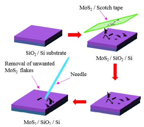
MoS2 flakes were obtained by exfoliation of bulk MoS2 (HQ graphene, high grade) with a strip of nitto tape(Fig. 1). The strip is folded several times in different angles with itself until the bulk MoS2 is spread over a defined area of the tape. From the used tape some of the cleaved bulk MoS2 flakes are transferred onto a new tape which is folded again several times with itself to cleave the MoS2 further more. This step can be repeated depending on the density of bulk MoS2 on the tape. The area of the last tape, also referred to as transfer tape in this work, which is covered by very thin layers of bulk MoS2 is then pressed onto the surface of the substrate before the tape is lifted off again very slowly. The substrate silicon covered by wet thermal oxidation of 3000ºA layer(Wafer mart, South Korea) is initially cleaned in acetone(high purity grade, Duksan Chemicals, South Korea), then into isopropanol(high purity grade, Duksan Chemicals, South Korea) and distilled water to get rid of any residues by ultra-sonication. These substrates containing MoS2 and bulk MoS2 were then scanned with an optical microscopy to locate the area of interest of MoS2 flake with 100x objective lens(Olympus BX51), the images were captured by CCD camera(Canon EOS-1D X), with the help of EOS utility software to store the images in the computer in auto exposures and auto white modes of 5184 × 3456 pixels.
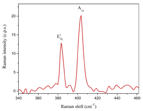
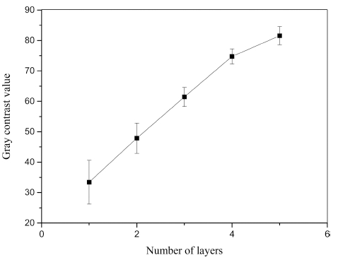
The MoS2 flakes(area of interest) must always be placed at the center of the image to get consistent results.23) In order to identify the number of layers, Raman spectroscopy( Thermo Scientific DXR) with 532 nm and full range grating was used and the data was saved in omnic software on the computer. The laser beam is focused onto the MoS2 samples by a 50x microscope objective lens and the images were detected using CCD detector. The Raman result indicates the E12g band and the A1g band shape of a peak for MoS2 whose difference varies with number of layers(Fig. 2). Number of layers were also measured using tapping mode AFM(XE 150, Park System, South Korea). The gray contrast values from low voltage FESEM(Gemini SEM 500, ZEISS) were calculated using the ImageJ(IJ 1.46r) software and Microsoft Excel 2013. Throughout the experiment, the working distance and the image resolution was maintained as 3 mm and 1024 × 768 pixels, respectively. The magnification and the scan time were adjusted depending on the size of the MoS2 flakes. The flakes’ thickness-induced contrast on SEM images are then correlated with the number of layers identified from the Raman spectroscopy and AFM data, in a graph format using the Origin software.
3. Results and Discussion
The number of layers of MoS2 flakes produced by mechanical exfoliation is uncontrollable. Thus, locating and identifying a single- or few-layered MoS2 flakes from all of the exfoliated flakes scattered on a vast substrate is essential, which is a time-consuming work. To identify the number of layers in multilayered MoS2, many methods have been proposed, which are discussed below. First TEM is a technique in which a beam of electrons interacts with the MoS2 sample as it passes through and accordingly the image is formed. But TEM needs MoS2 sheet samples suspended to ensure that optical absorption happens only in MoS2 and later after characterization it will no longer be useable.24)
AFM is a very-high-resolution type of scanning probe microscopy(SPM) with demonstrated resolution on the order of fractions of a nanometer. The machine gathers information by "feeling" or "touching" the surface with the help of a mechanical probe. There are piezoelectric elements which promote tiny but accurate and precise movements on scanning the area of interest.6,20,23,25,26) It is a very powerful and adaptable microscopy technique for the characterization of nanomaterials. It is used for various surface measurements and can provide a very high resolution topographic image. The AFM is one of the first techniques used to analyze graphene and other 2D materials but it also have some drawbacks. The single layer graphene observed under the AFM on oxidized wafers typically displayed the thickness to be 0.8~1.2 nm thick adding layer on top of it more than the expected 0.35 nm thickness, which is the actual thickness due to the van der Waals interlayer distance. According to Caterina et al, folded graphene or rough substrate might be the reasons for this additional height measurement but the reason is still unclear. In tapping mode AFM, graphene thickness measurement undergo from certain anomalies evoked by improperly chosen free amplitude values for the cantilever.27) Also AFM is time consuming and confined in lateral scanning so that it can be used as a primary method to determine the thickness of MoS2.28)
Raman spectroscopy is another tool to spot out the number of layers in multilayer MoS2. It avails monochromatic laser to connect with the molecular vibrational modes and the phonons in a sample, which shifts the laser photon energy down(stokes) or up(anti-stokes) through inelastic scattering. This energy shift generates two main peaks or the band in Raman spectrum: E12g(382 cm−1) and A1g(402 cm−1) in plane vibrational mode. The area cited are from a 532 nm excitation laser. Unlike in graphene, the 2D peak(band) shape change will occur as the number of layers of graphene increases into a wider, shorter higher frequency peak due to the added forces from the interactions between layers of AB-stacked graphene; this does not appear in MoS2. The difference between the E12g peak and A1g peak increases with number of layers with 1 unit. But the method is not full proof since doping and defects mostly complicates the spectra,29) making it challenging to differentiate the number of layers in multilayer MoS2. Also stack faults is a reason to avoid Raman spectroscopy as reported in.30) Further the peak difference is limited to only 4 layers(as shown in Fig. 3).6,20,31,32) Hence a close and careful examination of the peak difference is required in order to find the actual number of layers using Raman spectroscopy data.
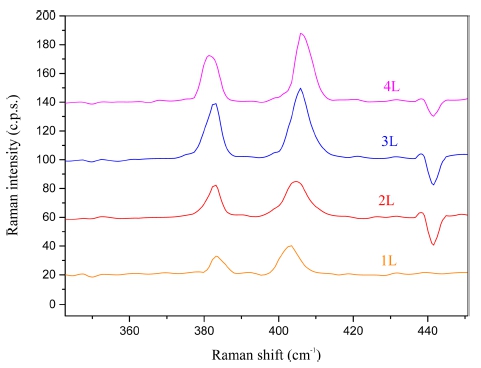
Fig. 3
Comparison of the difference in intensity of E12g band peak and A1g band peak on SiO2/Si substrates in Raman spectra as a function of number of layers for 532 nm excitation; E12g band ranges from 382-385 cm−1 and A1g band ranges from 402-406 cm−1.
Our previous RGB method23) using optical microscopy was a successful one for graphene, but it is applicable only on 100 to 300 nm thick SiO2 substrate.33) This method was extended to MoS2 flakes but when SEM images were taken for the same we found that SEM images produced high spatial resolution of MoS2 flakes and showed number of layers that are impossible to see with optical microscope image(Fig. 4). Also SEM images can clearly distinguish the number of MoS2 layers based on the contrast values. H. Hiura studied the mechanically exfoliated graphene flakes on SiO2/Si substrate with different number of layers by taking the SEM images from 0.5 kV to 20 kV.34) He also found a linear relationship between SEM contrast values and the number of graphene layers for 0.5, 1.0, 1.5, 3.0 and 10 kV. This method is applicable to flakes with less than 1 μm2 area which are not possible to see through optical microscopy. Further the method was extended to other insulating substrates like mica and sapphire. Hence this method is applied to MoS2 flakes on SiO2/Si substrate to obtain a linear relationship between SEM contrast values and number of MoS2 layers verified by AFM and Raman spectroscopy.
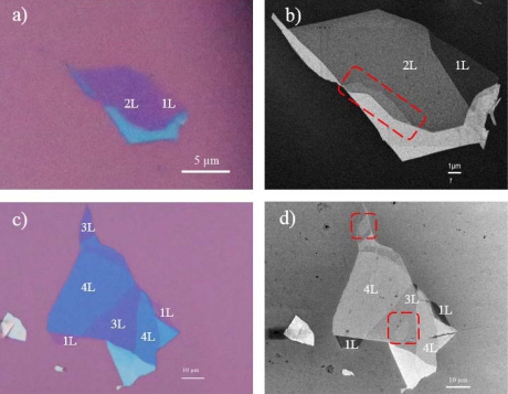
Fig. 4
(a) & (c) Optical image of MoS2 flakes with varying thickness on native SiO2/Si. The number of layers are marked my numerical (white color) that are verified by tapping mode AFM. (b) & (d) SEM images of MoS2 flakes corresponding to optical images (a) and (c) measured at 1 kV accelerating voltage. The contrast change with number of layers is clearly seen in the images. The dark grey color corresponds to monolayer MoS2 and the color becomes brighter with increasing MoS2 layers. The dotted red line depicts the MoS2 flake that are not visible in optical images (a) and (c).
The mechanically exfoliated MoS2 flakes on SiO2/Si substrate were measured using Raman spectroscopy and number of layers up to 4 were identified. Further to make a standard reference for the number of MoS2 layers, tapping mode AFM was used(Fig. 5). FESEM with low voltage of 1 kV was applied to capture the images of MoS2 flakes. Contrast values of each shade in the image which varied with number of MoS2 layers were obtained. The average contrast values along with standard deviation were then plotted against the standard reference of number of layers(Fig. 6). The linear relation shows that this method is reliable and can be rapidly used to identify the number of MoS2 layers. Further this method can be used to study other 2D materials like hexa-Boron Nitride (hBN), Tungsten diselenide(WSe2) etc.
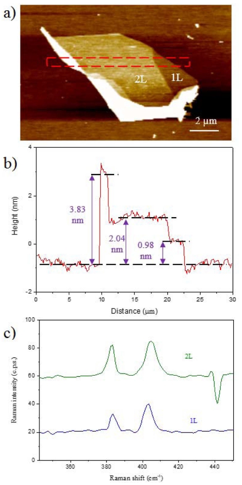
Fig. 5
(a) AFM image of MoS2 flake with mono, bi and bulk MoS2 layers. The dotted red line indicates the area of measurement. (b) Graph of measured area (red dotted line from Fig. 5(a)) showing the thickness of the flake by AFM. (c) Graph of measured area (red dotted line from Fig. 5(a)) showing the difference in intensity of E12g band peak and A1g band peak by Raman spectroscopy.
4. Conclusion
MoS2 flakes of various thicknesses were prepared on 300 nm thick-SiO2 substrate using mechanical exfoliation technique. The flakes were then observed by the Raman spectroscopy, AFM and low-voltage SEM, and the results were compared for one to five-layered flakes. We found that the AFM-determined number of layers exhibit a reasonably linear relationship with the corresponding SEM contrast. Also SEM can resolve the features too small to be discernable with optical microscopy. It is suggested that low voltage SEM can be effectively used with nano-level spatial resolution to identify the number of layers of MoS2 flakes on SiO2/Si substrate. Due to the high spatial resolution it can be further used to study the morphology of 2D materials.
