

1. Introduction
2. Experimental Procedure
3. Results and Discussion
3.1. Structural properties
3.2. Thermal Properties
3.3. Study of electrical properties
4. Conclusion
1. Introduction
When a material is cooled to a low temperature, depending on its type, the phenomenon of the disappearance of magnetic flux and electrical resistance within that material is known as superconductivity, and it is a significant phenomenon in solid-state physics.1) The temperature at which electrical resistance disappears is known as the critical temperature (Tc).2)
Superconductivity exhibits two key properties: magnetic behavior, which repels magnetic fields, and its electrical behavior, which exhibits zero electrical resistance to current. These two properties make superconducting materials highly sought after. Resistance to electrical current causes significant loss of electrical energy, overheating, and malfunction of many electrical devices. Magnetic fields continuously penetrate all ordinary materials without exception. However, magnetic fields cannot penetrate a superconductor while it is superconducting. Hence, when a material becomes superconducting, it acts as a perfect anti-magnet, repelling magnetic fields from within. This makes these materials revolutionary in various technologies and numerous applications.3,4)
Mercury-based superconductors are among the most important compounds, as they have the highest critical temperature. In 1993, the system (HgBa2Can-1CunO2n+2+δ) was discovered by Putilin et al.,5) resulting in a significant jump in the critical temperature of superconducting compounds. A critical temperature of 94 K was reached, and the structural formula was (HgBa2CuO4+δ). In the same year, Schilling et al.6) determined the structural formula (HgBa2Ca2Cu3O10+δ), with a critical temperature of 133 K.6,7) Chu noted that the pressure used in the compression inside the preparation furnace was important in raising the critical temperature, as the critical temperature of the compound (Hg-B-Ca-Cu-O) increased from 153 K to 160 K.6)
The BBCCO system is considered one of the most important high-temperature superconducting (HTSC) systems. The components of this superconducting ceramic system are bismuth oxide (BiO), barium oxide (BaO), calcium oxide (CaO), and copper oxide (CuO). HTSC is considered an important point in superconducting systems with a high critical transition temperature. The bismuth-based system has a general formula of (Bi2Ba2CanCun+1O2n+6) where n represents a positive integer (n = 0, 1, 2), so this system consists of groups of layers of copper oxide, each group separated by a calcium atom without oxygen. The interlocking layers of bismuth suboxide and barium oxide stabilize the copper oxide layers, so the first member of this family is 2201 with an octahedral copper oxide lattice, Tc = 20 K. The second member of this family is 2212, which has an n = 1 lattice and Tc = 90 K and has a single calcium layer. There are two layers of copper oxide, between which there is a calcium layer and the distance between the calcium and the copper oxide is 1.66 Å. The third member in this system is 2223 with an n = 2 lattice and three layers of copper oxide separated by calcium layers, with Tc = 110 K.8,9,10)
This system also includes three distinct phases: Bi-2201, Bi-2212, and Bi-2223. Two phases (Bi-2223 and Bi-2212) are considered most important because the boiling point of liquid nitrogen is more than its critical temperature. Starting with yttrium-based compounds and then bismuth-based compounds, these are superconductors with important applications.11,12) Among the advantages of this system are its environmental friendliness compared to mercury and thallium systems, as well as its high critical current, water resistance, high critical temperatures, and the purity and abundance of the elements from which the superconductor operates. Furthermore, it can withstand high magnetic fields more than other systems.13) Despite all these advantages, obtaining ideal growth conditions remains a challenging task.
The preparation of single-phase Bi2Ba2Ca1Cu3O10+δ materials is very difficult because phase 2223 is less thermodynamically favorable at high temperatures than phase 2212,14) and the chemical composition of these homogeneous phases overlaps with each other. Stated differently, it is challenging to prepare any of them as a comprehensive single phase, particularly when it comes to the 2223 phase. It is obvious that the partial replacement of Bi+3 in the oxygen-deficient Bi-O layer by cations with higher oxidation states of La+3, Zn, Cd+2, Pb+4, Cu+3, and Sb+3 makes the synthesis of a single-phase material easier and improves the stability.14,15,16,17,18) Moreover, the synthesis of (Tl, Sb) based materials has been emphasized because Sb can lower the melting temperature, increase the superconductivity transition temperature, stabilize the superconducting phase, and introduce more oxygen into the crystal structures.19) Replacing barium (Ba) with antimony and strontium can improve the hole doping in the copper (II) oxide interlayer, and a small addition of Sb can stabilize the flux in high magnetic fields, improving the critical intergranular current density.20,21) Chemical substitution of yttrium in Bi-2223 superconductors or Cu sites is also thought to make the insulation layer between copper (II) oxide interphase more metallic.22,23) Replacing Ba with the lower mass Sr cation enhances the interlayer coupling strength and shifts the non-reflection line to higher fields, causing the distance between the two superconducting copper (II) oxide phases to decrease. Lasers allow for precise and localized changes in the properties of superconductors. By applying focused energy, the crystal structure and charge distribution can be modified, affecting their microstructure and electrical properties, and enabling the design and development of new materials with improved performance in various applications. This paper includes an explanation and discussion of the results of the laser beam effect on the structural, electrical, and thermal properties of an HTSC compound with the chemical formula Bi1.9Sb0.1Ba1.9Y0.1Ca2Cu3O10+δ, which was prepared by a solid-state reaction at an annealing temperature of 900 °C with a hydrostatic pressure of 7 MPa.
2. Experimental Procedure
The Bi1.9Sb0.1Ba1.9Y0.1Ca2Cu3O10+δ samples were prepared from high-purity oxide powders (Bi2O3, BaO, CaO, CuO, Sb2O3 and Y2O3). Appropriate weights of these highly pure powders (99.99 %) samples were prepared using the solid-state reaction (SSR) method, as in the chemical formula below:
0.95 Bi2O3 + 0.1 Sb + 1.9 BaO + 0.1 Y2O3 + 2 CaO + 3 CuO → Bi1.9Sb0.1Ba1.9Y0.1Ca2Cu3O10+δ
The powders were mixed and ground using an agate mortar, then pressed under a hydrostatic pressure of 7 MPa for 3 minutes to obtain discs with a diameter of 1.5 cm and a thickness of 2.5-2.8 mm. The samples were placed in an electric furnace to form the superconducting compound. The furnace temperature was raised to 900 °C at a heating rate of 10 °C/min. The samples were kept at this temperature for 48 h, after which the furnace temperature was lowered to room temperature at the same heating rate.
The samples were cleaned and polished, and their structural properties were then examined using a Shimadzu Cu Kα X-ray spectrometer at 40 kV, 30 mA, and a wavelength of 1.5406 Å. The ratios of the samples (2θ, d, hkl, and I) were determined. After examining the samples and comparing them to its counterparts in standard tests, the resulting phases (Bi-2223) were identified. We then used computational algorithms to calculate the lattice parameters per unit cell, as well as the lattice constants a, b, and c, using Bragg’s law of X-ray diffraction.24,25) After determining the relationship between a, b, and c using X’Pert HighScore Plus software, the atomic dimensions of the crystal structure could be determined. Scanning electron microscopy (SEM) was used to examine the surface of the samples. High-resolution images with magnifications up to 100,000× could be obtained anywhere on the sample surface, depending on the interaction of electrons with the material. The samples were analyzed using energy-dispersive X-ray spectroscopy (EDX) to confirm the proportions of their constituent elements. Additionally, a Li disk was used to study the thermal conductivity of the samples before and after laser irradiation.
3. Results and Discussion
3.1. Structural properties
3.1.1. Energy-Dispersive X-ray spectroscopy (EDX)
EDX was used to analyze the elements and determine the chemical properties of the sample. EDX is an analytical technique used to determine the type and quantity of chemical elements in a sample and the sample’s chemical properties. This technique involves bombarding the sample with a high-energy electron beam, causing the inner electrons to emit and creating voids. When outer electrons fill these voids, they emit X-rays at energy levels characteristic of each element, allowing for precise identification and quantification of the elements.26) The vacancies in the upper atomic orbitals are subsequently filled by the electron that is emitted from the inner atomic orbitals, which causes excitation and instability.27,28) The atomic orbitals of the electrons that formed the vacancy with the electron that filled it will determine that each element has a restricted quantity of permitted atomic orbital transitions. Kα, Kβ, Lα, and other symbols represent these paths (lines) or transitions, which are referred to as transition quantum numbers when the X-ray photon is absorbed within the sensitive region and measures the energy of the photons by the detector. This results in a proportionate number of electrons being amplified in the resulting spectrum, which is used to create a quantitative standard that uses an indicator to provide a value that appears on the x-axis as an energy value. As shown in Fig. 1 and Table 1, which display the EDX analysis of the samples as well as the elemental ratios in the compound, it was proven that the results were completely consistent with the samples’ composition. In addition to the antimony and yttrium elements, the results demonstrated the presence of the primary constituents of the compound, indicating its purity and the precise weight compensation used during sample preparation.29,30)
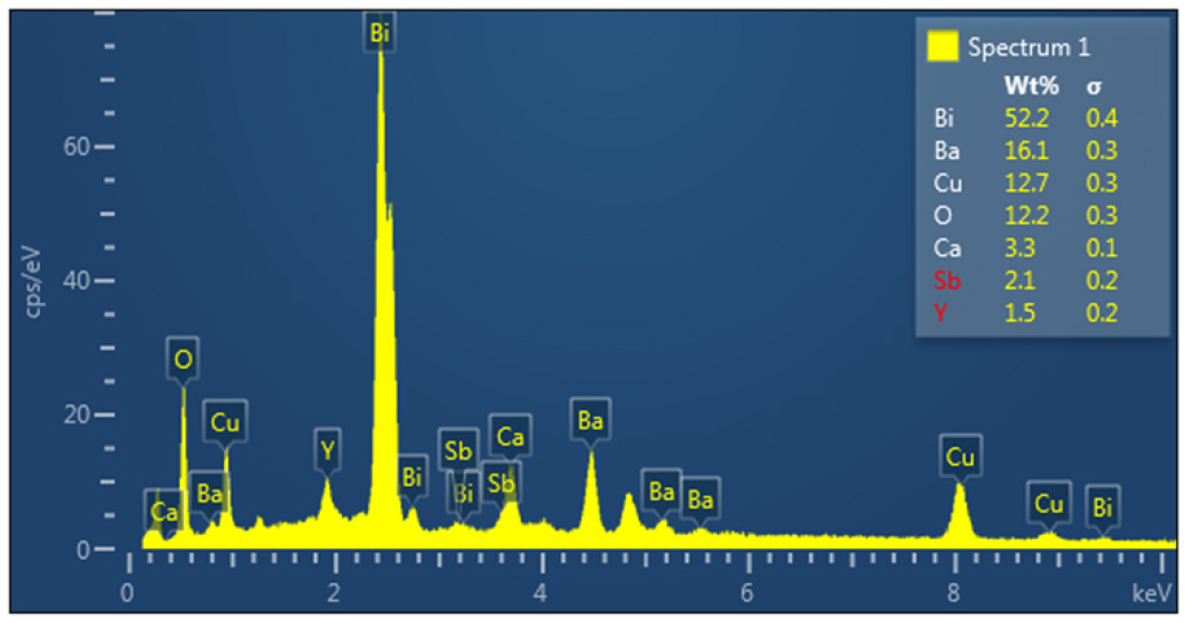
Table 1.
Concentrations , Line Type and Atomic of chemical elements for Bi1.9Sb0.1Ba1.9Y0.1Ca2Cu3O10+δ compound.
3.1.2. XRD analysis
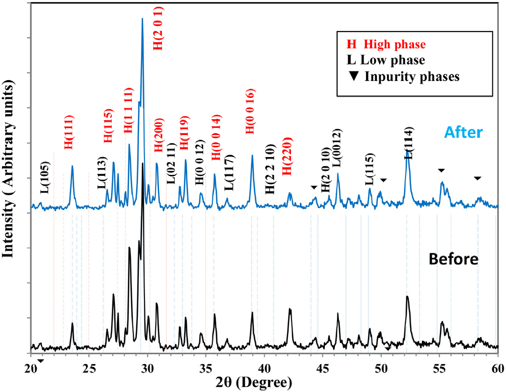
The XRD analysis of Bi1.9Sb0.1Ba1.9Y0.1Ca2Cu3O10+δ superconducting compound prepared by the SSR method at temperature of 900 °C and pressure (7 ton/cm2), partially substituted with nano-antimony oxide Sb2O3 in the bismuth element at ratios (Sb = 0.1) before and after laser irradiation. This study showed that the samples had two phases and a regular crystal structure (the main high-temperature phase Bi-2223 and the low-temperature phase Bi-2212 phases) and that the proportions of the phases change according to the effect of laser radiation, in addition to the appearance of other impurities, as shown in Fig. 2. The intensity of the high-phase peaks (Bi-2223) is observed to be greater than that of the peaks (Bi-2212) and other phases. Therefore, the longer the heat treatment period (sintering and annealing), the greater the intensity of the high-phase peaks and the closer they approach the monoclinic phase of the compound. This is because the alignment of positive ions, changes in oxygen content, and atomic alignment along the c-axis are affected by changes in the atomic structure, which in turn leads to changes in the crystal structure. The sample exhibits different phases as a result of these combined factors.31,32) XRD data were entered into the X’Pert HighScore Plus software to calculate Miller indices (hkl) and lattice constants (a, b, c) and to determine the best match between the Bi1.9Sb0.1Ba1.9Y0.1Ca2Cu3O10+δ composite samples. The results showed that all samples possessed an orthorhombic crystal system. After identifying the peaks, their intensity, and types in each sample before and after laser irradiation, the phase ratios, lattice constants, theoretical unit cell densities, and (c/a) values were calculated and are presented in Table 2. It is evident from the table that the recorded values change after laser irradiation. The reason is that the effect of radiation and the duration of sample retention raise the temperature, as they play a role in giving more energy and a longer time to the transported masses, which facilitates the reaction process between the atoms of the elements that make up the compound, leading to molecular interference.31) Also, the freedom of movement of molecules and atoms during the sample’s exposure to radiation leads to the introduction of copper oxide layers, which increases the concentration of the higher phase. It aims to shorten the molecular distances based on their size, which prolongs their duration to achieve balanced thermodynamic phases. It also adds more CuO layers to the low-phase structures, which promotes the formation of the high-phase.33) XRD results showed a marked increase in the intensity of the high-phase peaks, and a corresponding increase in the proportion of high-temperature phase (HTP) from 77.32 % before the laser effect to 81.47 % after the effect. The laser effect also contributed to an increase in the length of the c-axis from 36.4969 Å before the effect to 36.577 Å after the laser effect, and the c/a ratio also increased from 6.739 to 6.770.
Table 2.
Lattice constants, the density, the ratio (c/a), and the proportion of the higher phase of the Bi1.9Sb0.1Ba1.9Y0.1Ca2Cu3O10+δ compound before and after laser radiation.
| Laser irradiation | a (Å) | b (Å) | c (Å) | c/a | V (Å3) | ρm (g/cm3) | High-Tc phase (%) |
| Before | 5.4157 | 5.4317 | 36.4969 | 6.739 | 1073.605 | 5.649 | 77.32 % |
| After | 5.4018 | 5.4843 | 36.5677 | 6.770 | 1083.319 | 5.505 | 81.47 % |
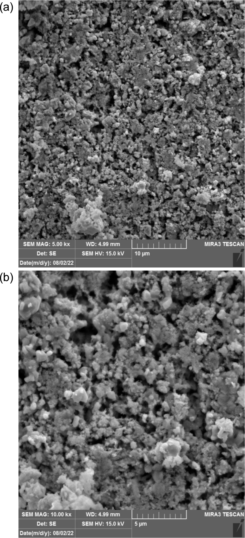
3.1.3. Study the surface microstructure
The superconducting compound was examined for its composition and morphology. Where the concentration of nano-yttrium oxide (y = 0.1) and the concentration ratio of nano-antimony oxide (x = 0.1) were fixed. Using the SEM technique, each concentration was represented by an image at a magnification power of 5.00 kx and 10.00 kx and higher. As seen in Fig. 3 (a, b), which shows the SEM analysis of the sample both before and after laser irradiation, exposure shows the development of a grain size with measurements ranging from 86.65 to 97.32 nm. The images’ results demonstrated the two samples’ obvious homogeneity since they showed bright spots that represented sizable portions of the sample surface and were indicative of the compound’s oxides of light elements such as (Ca) are represented by dark areas, while the oxides of heavy elements such as bismuth (Bi) and copper oxide (CuO) improve the critical temperature of the samples. The results after irradiation revealed the formation of new phases, a change in size, and smaller grain sizes than in the composite sample before irradiation. The reduced grain size increases the area of the grain boundaries, which aids the movement of current carriers in the process of superconductivity, and the formation of new phases and different grain sizes.34) The difference continues in the spread of light areas and grain size.35)
3.2. Thermal Properties
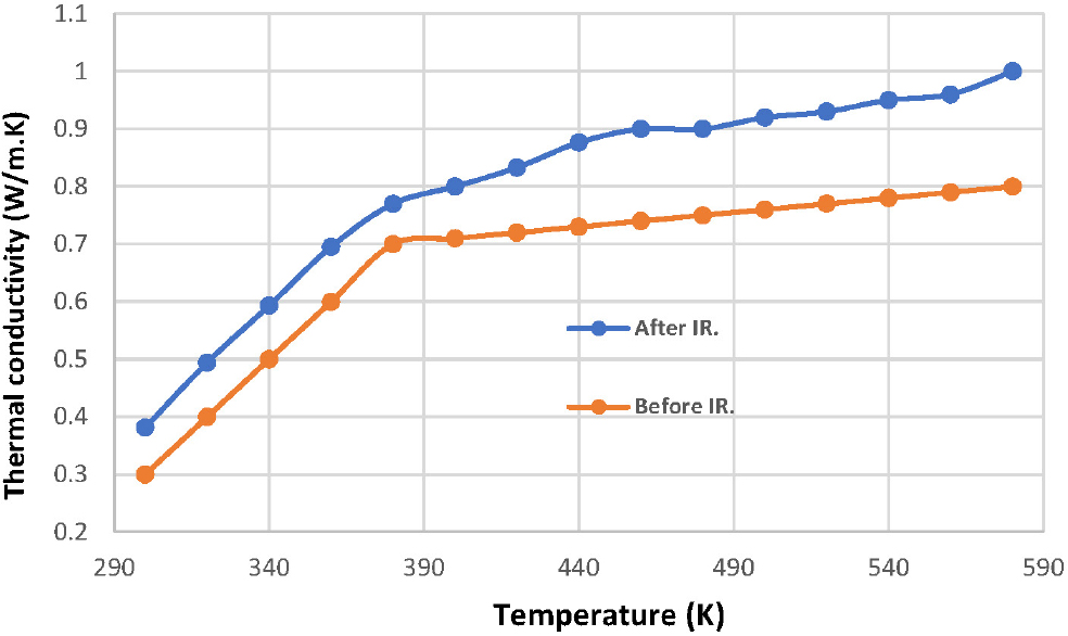
The thermal properties of the Bi1.9Sb0.1Ba1.9Y0.1Ca2Cu3O10+δ compound, partially substituted with nano-antimony oxide (Sb2O3) and nano-yttrium oxide (Y2O3), were studied. The thermal conductivity of the samples was measured using a Lee disc device before and after laser irradiation. Fig. 4 shows the thermal conductivity of the compound as a function of temperature. It is observed that the thermal conductivity of the two samples increased with increasing temperature, both before and after irradiation. The results showed an improvement in the thermal conductivity of the irradiated sample compared to the unirradiated sample. It also notes that the conductivity varies in some regions of the curve; this suggests that laser irradiation has created a continuous bond between the atoms,36) which leads to an increase in temperature. The lattice vibration also depends on the phonon energy; as the phonon energy increases, so does the lattice vibration, leading to an increase in thermal conductivity.37)
3.3. Study of electrical properties
The electrical properties of the superconducting compound were studied before and after laser irradiation. Fig. 5 illustrates the relationship between temperature and DC resistance. Both samples exhibited metallic behavior, with resistance decreasing as temperature decreased, and the slope of the two curves differed. From the resistivity curve in Fig. 5, values of the critical temperatures (Tc(offset)) (at zero resistivity) and when the electrical resistance begins to drop [critical operating temperature Tc(onset)] before and after irradiation with fluxes can be obtained. These temperatures were found to be 110 K before, 114 K after irradiation for Tc(offset) and 126 K and 131 K for [Tc(onset)], respectively. This phenomenon is manifested by sharp drops in electrical resistivity at the superconducting onset temperatures [Tc(onset)]. The superconducting onset temperatures of the samples before and after laser irradiation were observed at approximately 126 K and 131 K, respectively. In contrast, zero electrical resistance was reached at approximately 110 K and 114 K, respectively. The transition bandwidth was approximately 16 K and 17 K, respectively, indicating that the transitions are semi-sharp and well-defined. The electrical resistance measurements indicate that the materials are stable, thermally recyclable, and reproducible. As previously mentioned, the samples exhibit metallic conductive behavior from room temperature up to the superconducting transition temperatures. The granular superconductors, with their well-defined superconducting transition temperatures, generally exhibit a visible phase, and the rate of change in resistance shows its peak on the lower end of the critical operating temperature [Tc(onset)].
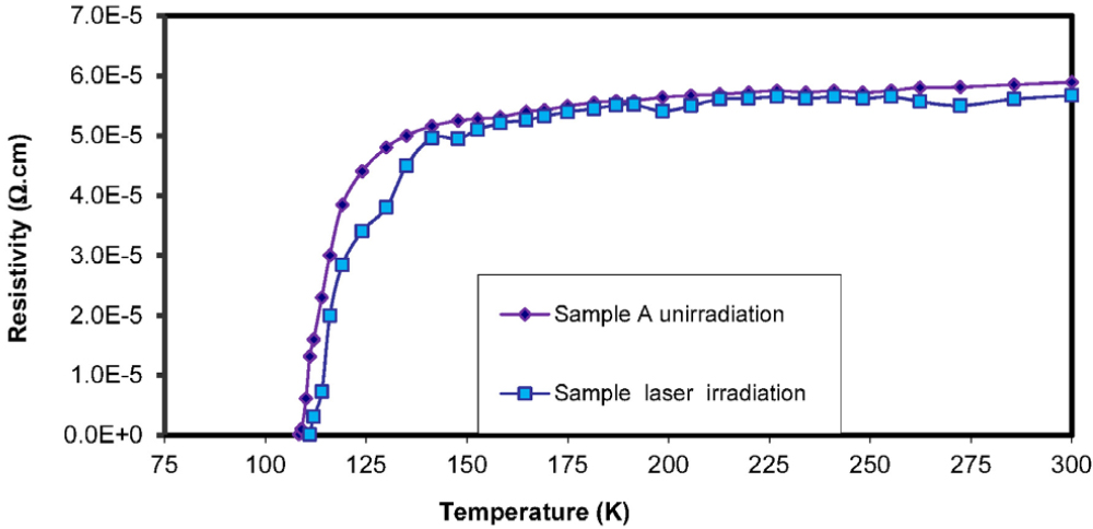
Changes in oxygen content are the cause of the apparent behavior.38,39) It regulates the number of holes in the layers of copper oxide. As a result, radiation naturally alters the oxygen content, which may alter the concentration of carriers and raise the measured Tc values. Laser radiation may damage weak bonds between grains and realign them due to the high heat absorbed by the samples.40,41) The critical transition temperature rises because radiation likely causes defects, which increase the number of holes in the lattice, Tc, by creating flaws and rupturing links in CuO planes.42,43) The results showed that the critical temperature Tc value varied for the samples depending on the effect of radiation, as shown in Table 3, which represents the essential temperature values for each sample before and after radiation.
4. Conclusion
In this research, we studied the physical properties of superconductors and the effect of laser radiation on Bi1.9Sb0.1Ba1.9Y0.1Ca2Cu3O10+δ synthesized by a conventional (SSR) method. The transition temperatures of the radiation-sensitive cultured samples increased from 110 K before irradiation to 114 K after irradiation. The change in Tc can be explained by the movement of smaller defects and their interaction with radiation-induced defects. The lattice parameter c/a ratio, volume fraction, and oxygen content were found to change with irradiation. The observed shift in c/a ratio is the reason for the significant increase in the volume fraction, which supports the possibility that the displacement of oxygen atoms in the CuO chains. Since the irradiation effect may also lead to the formation of effective stabilization centers, it is desirable to investigate the use of radiation in the development of the flow stabilization mechanism.
