

1. Introduction
Metal-semiconductor(MS) contacts are essential elements in modern electronic and optoelectronic applications such as gate electrodes of a metal-semiconductor field-effect transistor(MESFET), the drain and source contacts in metal-oxide-semiconductor field-effect transistor(MOSFET) and contact electrodes in solar cells, high electron mobility transistors(HEMTs) and light emitting diodes (LEDs). The current transport across the Schottky contacts is mainly due to majority carriers and the barrier height is an important parameter that determines the electrical characteristics of MS contacts. In practical Schottky diode, the interfacial region of a Schottky barrier is not spatially homogeneous and edge effects at the perimeter of the diode become important. Distinguishing between bulk and perimeter currents has been used to analyze current-voltage characteristics of GaN diodes,1) GaInAsSb based photodetectors2) and polymer light emitting diodes.3) Such devices indicate that bulk current becomes more important with respect to the perimeter current as the contact area increases. Using the simulation, it was shown in Al/GaAs diode that the ratio of leakage to non-leakage current at low forward bias region increased with decreasing contact area and was associated with the enhanced tunneling current.4)
As an alternative channel material for high-speed complementary metal-oxide-semiconductor(CMOS) devices, Ge has gained considerable interest due to its high electron and hole mobilities.5-11) In ultra-scaled Ge based devices, very low resistance is required. However, the barrier height in n-Ge is inevitably high due to strong Fermi level pinning, leading to high device resistance.5) Additionally, in a very large scale integration(VLSI) application, it is important to obtain high-level uniformity in the electrical properties across a large area wafer. For such application, metal contacts with different areas may be incorporated into the same device. As far as we know, there is not much work on the investigation of detailed current transport mechanisms in Ge based Schottky diodes using different contact areas. In this work, we fabricated Au Schottky contacts to n-type Ge and the relevant contact area dependence of electrical properties was investigated.
2. Experimental
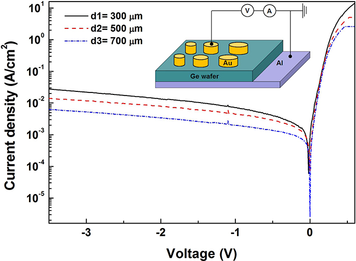
In this work, we used single-side-polished Sb-doped Ge (100) wafer (thickness of 500 μm and carrier concentration of ~1 × 1016 cm−3) as an investigation material. After solvent cleaning, Au Schottky contacts with a thickness of 100 nm were deposited by radio-frequency (RF) magnetron sputtering through a shadow mask onto the polished side of the Ge wafer. The diameters of the Schottky contacts were 300, 500 and 700 μm, which were denoted as d1, d2 and d3 samples, respectively. Then, Al metal with a thickness of 150 nm was deposited as an ohmic contact over the entire back surface of the sample. The schematic structure of the fabricated Au/n- Ge Schottky diode is shown in the inset of Fig. 1. Current-voltage (I-V) measurements were carried out at room temperature with a Keithley 238 current source.
3. Results and Discussion
Fig. 1 shows the typical semi-logarithmic current density vs. voltage (J-V) curves for three samples. The current densities are expected to be similar but there exist the differences in the J-V data, indicating that the current transport at the perimeter of the contact is not negligible. Reverse bias I-V curves can be analyzed using the form ln(I) vs. V1/2, by considering either a Schottky or a Poole- Frenkel effect.12)
where d is the depletion width and βS and βPF are the Schottky and Poole-Frenkel emission coefficients, respectively, given as 2βS=βPF=(e3/πεSε0)1/2. Using εS = 16.0 for Ge, the theoretical values of βS and βPF were calculated to be 9.50 × 10⁻⁶ and 1.90 × 10⁻⁵Vm1/2V−1/2, respectively. The experimental emission coefficients were obtained by plotting the reverse-bias I-V characteristics in the form of ln(I) vs. V1/2 shown in Fig. 2. The emission coefficients calculated from the linear portions of the curves are shown in the inset of Fig. 2. Here, the numbers ‘1’ and ‘2’ on the lines represent the theoretical values of βS and βPF, respectively. For three samples, the experimental values obtained were closer to the values for Poole-Frenkel emission. Poole-Frenkel emission was dominant in the lower voltage region, in which carrier transport from the metal contact into the conductive states must occur via trapped states rather than by direct thermionic emission from the metal.13) From these results, it can be inferred that for d1 sample the structural defect or nonuniformity of the interfacial layer can increase the reverse leakage current.
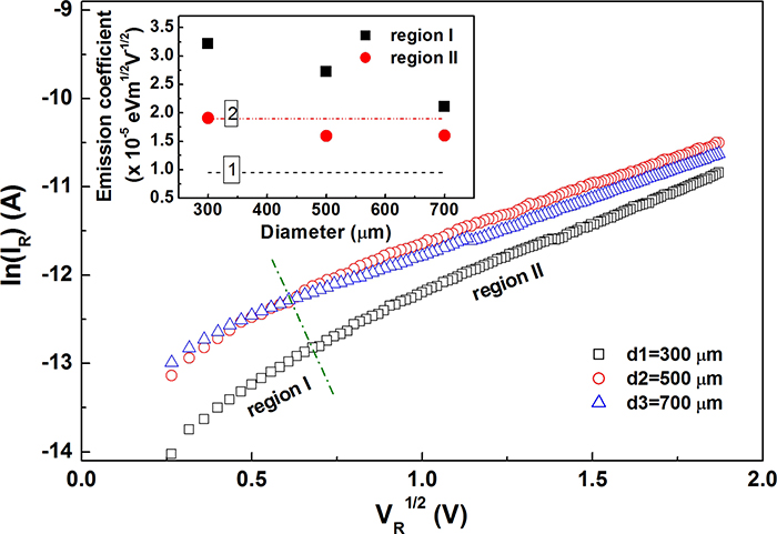
Fig. 2.
Plots of ln(IR) versus V1/2. The inset shows the experimental emission coefficients and the numbered lines ‘1’ and ‘2’ denote the theoretical Schottky and Poole-Frenkel emission coefficients, respectively.
The dependence of the leakage currents on the Schottky electrode size was analyzed to clarify the dominant current component of the reverse leakage current. The reverse leakage current can be assumed to be a sum of a bulk current uniformly flowing over the Schottky electrode and a perimeter current flowing around at the periphery of the Schottky electrode, which is given by14)
where A(cm2) is the diode area, JB(A/cm2) is the bulk current density, P(cm) is the length of the diode perimeter, and JP(A/cm) is the perimeter current density. Using the linear fit to I⁄A vs. P⁄A plot as shown in Fig. 3, we can obtain JB and JP values from the intercept and the slope, respectively. The inset in Fig. 3 shows the obtained JB and JP values at different reverse bias voltages. The JB values are almost constant below −2 V and then decreases with increasing reverse bias. The JP values increase monotonically with increasing reverse bias and the slope becomes larger above −2 V. The contribution of JP to reverse leakage current becomes high at high reverse bias voltage, which probably results from the tunneling at the perimeter of the electrode.
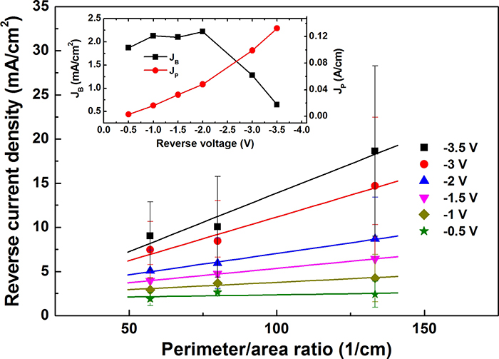
Fig. 3.
Reverse leakage current density vs. perimeter/area ratio. The inset shows the obtained bulk current density (JB) and the perimeter current density (JP) values at different reverse bias voltages.
The Schottky barrier heights(SBHs, φB) and the ideality factors were determined from the forward bias I-V curves based on the thermionic emission(TE) model.15) The forward I-V analyses revealed that φB = 0.59(± 0.01), 0.58(± 0.02) and 0.61(± 0.01) eV for d1, d2 and d3 samples, respectively. The ideality factors were found to be 1.49(± 0.07), 1.49(± 0.16) and 1.37(± 0.05) for d1, d2 and d3 samples, respectively. Compared to d1 and d2 samples, d3 sample showed lower ideality factor(though the difference is not significant). In order to explain the extracted electrical parameters in more detail, the forward bias current transport in Au/n-Ge Schottky diodes were analyzed using various transport components. The total current ITOT(ITOT = ITE + IGR + ITU + ILE) can be assumed to be the sum of different transport mechanisms.16,17) Here, ITE is the TE current, IGR is the generation-recombination( GR) current, ITU is the tunneling current and ILE is the leakage current. The TE current is
where ITE0 is the saturation current of the TE component and RS is the series resistance. The series resistance(RS) values were extracted from the curves where the I-V data begin to saturate. The GR current is
where IGR0 is the saturation current of the GR component. The tunneling current is
where ITU0 is the saturation current of the tunneling component and E0 = E00 coth(E00/kT) is a parameter dependent on barrier transparency (E00 is the characteristic energy related to the tunneling probability). Note that the contribution of leakage current to total current was negligibly small, so it was not considered for the fitting.
Fitting to experimental I-V data with theoretical I-V curves was performed by considering ITE0, IGR0, ITU0 and E0 as fitting parameters. Comparison between the experimental and the fitted curves are shown in Fig. 4. For three samples, the I-V data were fitted better when the combination of TE, GR and tunneling currents was considered. The TE current and the tunneling currents are dominant at higher and lower forward bias region, respectively. The contribution of the GR current also cannot be negligible. Fig. 5(a) shows the obtained fitting parameters of ITE0, IGR0, ITU0. Both the ITE0 and IGR0 values increase with the contact area whereas the ITU0 value is almost constant. As shown in Fig. 5(b), these values were compared after dividing by contact area. The variations of both the JTE0 and JGR0 values with the contact area are small. However, the decrease of JTU0 values with the contact area is seen clearly. This indicates that both the TE and GR currents mainly flow through the bulk region and the enhanced tunneling current at small contact area is related with the current flow at the perimeter region of the electrode. From the obtained ITE0 values, the barrier heights were calculated to be 0.70, 0.69 and 0.69 eV for d1, d2 and d3 samples, respectively. The similar barrier heights for three samples indicate again that the TE current flows mainly through the bulk region. Compared to the barrier heights from I-V data, these barrier heights are higher. There exist regions of lower barrier height which are embedded in areas of larger barrier height in actual diodes, and this kind of barrier inhomogeneity reduced the effective barrier height for I-V data.
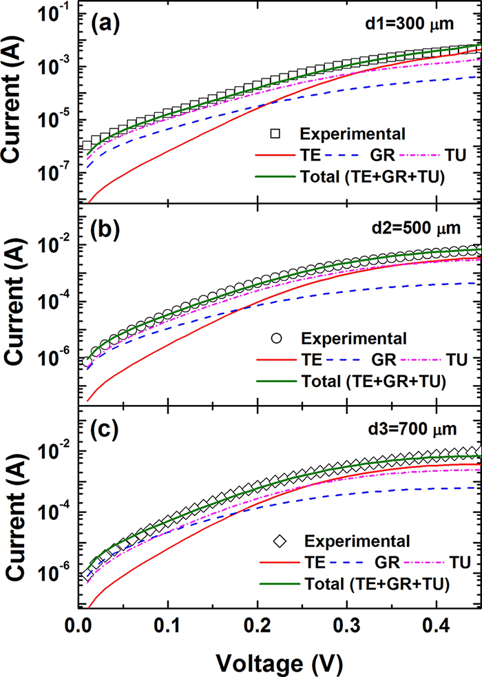
Fig. 4.
Fitting results of the forward bias current-voltage (I-V) characteristics of Au/n-Ge Schottky diodes for three samples.
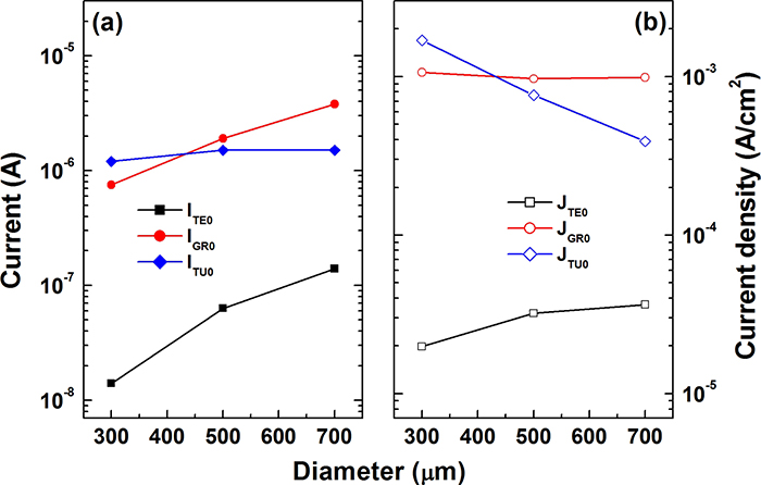
Fig. 5.
(a) Fitting parameters for theoretical I-V curves and (b) their current densities obtained by dividing the current values by contact area.
The E00 values related to tunneling probability were calculated as 41.6, 31.1 and 28.7 eV for d1, d2 and d3 samples, respectively. The current transport mechanism is dependent on the E00 value, such as TE for E00/kT<<1, thermionic field emission(TFE) for E00/kT~1, and field emission(FE) for E00/kT>>1.18) The E00/kT values for three samples lied between 1.1 and 1.6, indicating that the TFE is a dominant current transport. With decreasing contact area, the tunneling current increased at the perimeter of the contact, which in turn increased the ideality factor. Edge or perimeter current can result from defects and impurities induced during device production. Therefore, suppression of current paths due to the edge current is required to improve the device reliability.
4. Conclusion
Using current-voltage (I-V) measurements, we investigated the electrical properties of Au/n-type Ge Schottky contacts with different contact areas. From the analyses on the reverse bias current characteristics, it was found that Poole-Frenkel effect became strong with decreasing contact area. With increasing reverse bias voltage, the contribution of bulk current density(perimeter current density) to total current density was found to decrease (increase). From the fitting to forward bias I-V characteristics with considering various transport models, we found that the tunneling current is dominant at low forward bias region. The contribution of thermionic emission and generation-recombination currents to total current was similar regardless of the contact area. However, the contribution of tunneling current to total current was observed to increase with decreasing contact area. Hence, the current transport at the perimeter of the electrode mainly comes from the tunneling current.
