

1. Introduction
2. Experimental Procedure
2.1. ED AgNW TCE fabrication
2.2. CIGS device fabrication
2.3. Measurement of optoelectrical properties
3. Results and Discussion
4. Conclusion
1. Introduction
Transparent conducting electrodes (TCEs) represent integral components within various optoelectronic applications, prominently featuring solar cells, light-emitting diodes (LEDs), and liquid crystal displays (LCDs).1,2,3) Ongoing global research endeavors are focused on refining the manufacturing methodologies of TCEs, aiming to augment the operational efficiency and efficacy of these optoelectronic systems.4)
Indium tin oxide (ITO) thin films, fabricated via pulsed laser deposition, ion beam sputtering, electrostatic spray-assisted vapor deposition, and magnetron sputtering, exemplify a TCE widely employed in optoelectronic devices due to its superior transparency and low sheet resistance.5,6,7,8,9) Despite these desirable properties, the prohibitive cost associated with ITO thin films has spurred investigations into carbon nanotubes, graphene, and metal nanowires as alternative TCE materials.10,11,12,13,14,15,16) Among these alternatives, silver nanowires (AgNWs) have emerged as particularly promising, owing to their reduced processing time and cost. Furthermore, AgNWs have demonstrated exceptional suitability for flexible electronics. Notably, Park et al.17) observed no instances of cracking or delamination in AgNW-based devices subjected to 10,000 cycles of bending, both inward and outward. Consequently, AgNWs exhibit considerable potential for integration into flexible and wearable optoelectronic platforms.
The optical and electrical characteristics of AgNWs have been extensively studied by numerous researchers employing theoretical models and experimental techniques.18,19,20,21) The sheet resistance (Rs) of AgNW networks is notably influenced by both the length as well as areal density of the nanowires, while the transmittance (T) exhibits an inverse relationship with the areal density of the AgNW network.22) Notably, when the diameter of AgNWs falls below 30 nm, the T and Rs of the AgNW network closely resemble those of ITO.23,24) However, AgNWs with such reduced diameters are susceptible to stability issues. To mitigate these concerns, a strategy involving silver (Ag) electrodeposition onto the AgNW TCE has been introduced. This approach effectively enhances the stability and conductivity of the TCE by enlarging the diameter of AgNWs and facilitating the welding of AgNW-to-AgNW junctions.25)
The optoelectrical characteristics of electrodeposited (ED) AgNW TCEs can be effectively modulated through variations in electrodeposition time. This study offers an in-depth examination of the optical and electrical attributes of AgNW TCEs as a function of increasing electrodeposition durations. To assess the efficacy of the TCEs with the ED AgNW network, the figure of merit (FoM) is utilized, with its evaluation conducted across varying electrodeposition periods. Furthermore, to ascertain the improvements in optoelectrical properties, stability, and reliability conferred by the Ag electrodeposition procedure, the integration of Ag ED AgNW TCEs into Cu(In,Ga)Se2 (CIGS) solar cells is demonstrated, with a thorough investigation into their resultant performance.
2. Experimental Procedure
2.1. ED AgNW TCE fabrication
A suspension of AgNWs at a concentration of 1 mg/mL was prepared utilizing AgNWs characterized by an average diameter of approximately 45 and 80 nm, with lengths spanning from 100 to 200 µm. This suspension was then spin-coated onto glass substrates measuring 25 mm × 25 mm, employing spin coating at 1,000 rpm for 30 s. After the spin coating process, a network comprising AgNWs was established on the glass substrate, serving as the working electrode for electrodeposition. Counter electrode duties were fulfilled by Ag foil. The electrolyte utilized for Ag electrodeposition was formulated with 70 g/L silver cyanide (AgCN), 15 g/L potassium carbonate (K2CO3), 150 g/L potassium cyanide (KCN), and 50 g/L sodium thiosulfate (Na2S2O3), with AgCN serving as the Ag precursor and the remaining constituents acting as buffers. Employing a potentiostat, a constant current density of 1 mA/cm2 was maintained between the electrodes for a duration of up to 20 s at room temperature to facilitate Ag electrodeposition onto the spin-coated AgNW network. A comprehensive description of the fabrication process is also available in another source.25)
2.2. CIGS device fabrication
The CIGS thin-film solar cells were structured as TCE/CdS/CIGS/Mo/Glass. The construction involved the deposition of absorber layers comprising indium (In), gallium (Ga), selenium (Se), and copper (Cu) with a combined thickness of 2 µm via a three-stage co-evaporation technique onto glass substrates coated with molybdenum (Mo). Subsequently, a CdS buffer layer of 50 nm thickness was deposited on the CIGS thin film through chemical bath deposition. Following this, spin-coating of AgNW TCEs was carried out, succeeded by an electrodeposition process. A detailed account of the fabrication procedure can be found elsewhere.26)
2.3. Measurement of optoelectrical properties
The ultraviolet-visible spectrophotometer was employed to record the total transmittance (Ttotal) and specular transmittance (Tspecular) spectra of both the as-spin-coated and ED AgNW TCEs, utilizing a glass substrate as the reference material. The Rs of the AgNW TCEs was determined utilizing a four-point probe station. Furthermore, the J-V characteristics of CIGS solar cells featuring the TCE/CdS/CIGS/Mo/Glass configuration were assessed using a solar simulator operating under the illumination of a 1,000 W/m2 AM 1.5G spectrum, with measurements conducted via a source meter (Keithley 2401).
3. Results and Discussion
The Ttotal of a material can be deconstructed into two distinct components: Tspecular and diffuse transmittance (Tdiffuse). Tspecular refers to the portion of transmitted radiation collected by a detector aligned with the incident radiation axis. Conversely, Tdiffuse entails the collection of transmitted light across all angles. Consequently, the Ttotal is mathematically represented by Eq. (1).
Haze, a parameter indicative of light scattering within a material, can be quantified by computing the ratio of Tdiffuse to Ttotal. This relationship can be expressed through the utilization of specific mathematical Eqs. (2) and (3).
Fig. 1(a, b) present the total and Tspecular data obtained over a wavelength range of 350 nm to 1,100 nm for the TCE. Fig. 1(c) illustrates the corresponding Haze values computed across varying Ag electrodeposition durations ranging from 0 to 80 s. As the electrodeposition time increases, there is a notable augmentation in the obstruction and scattering of incident light attributable to the expanded area and heightened surface roughness of AgNWs. Consequently, both Ttotal and Tspecular exhibit a decline. This decline corresponds to an elevation in haze values with increasing electrodeposition time.
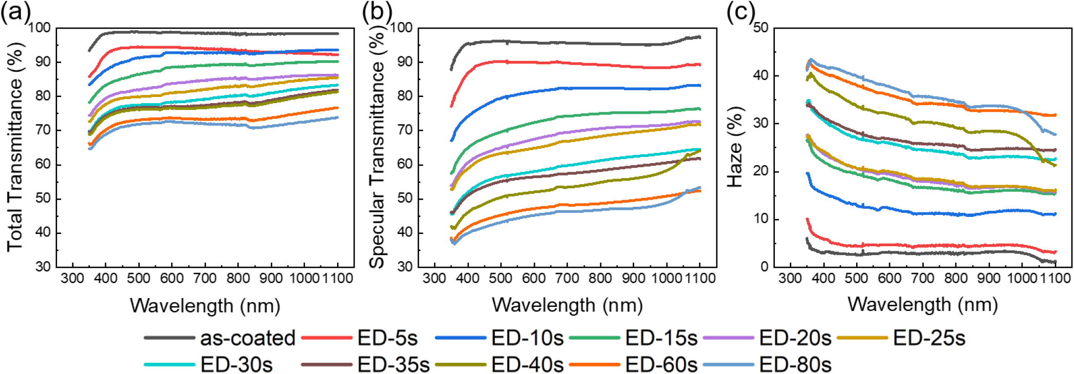
Fig. 2(a) illustrates the Ttotal, Tspecular, and haze characteristics of the TCE at a wavelength of 550 nm, aligning with the peak sensitivity of the human eye according to the luminosity function, across different electrodeposition durations. This figure provides insights into the alterations observed in these optical parameters of AgNWs TCEs as a function of increasing electrodeposition time. Specifically, the Ttotal decreased from 98.71 % to 72.28 %, and the Tspecular decreased from 95.95 % to 44.33 % as the electrodeposition time increased from 0 to 80 s. Consequently, the haze of the AgNWs TCE increased from 2.79 % to 38.66 % over the same electrodeposition time range.
To examine the impact of extended electrodeposition time on the T, let us assume a square lattice structure of the nanonetwork as shown in Fig. 2(b). For which T can be calculated using the Eq. (4).25)
where, L is the spacing between nanowires, and D is the diameter of the nanowires. The desired T value can be achieved by regulating the diameter of AgNW, which is controlled by adjusting the electrodeposition time.
Fig. 2(c) illustrates the relative variation of Haze and Ttotal with increasing electrodeposition time, which is calculated using the Eqs. (5) and (6).27)
where, HED-AgNW and TED-AgNW represent the haze and Ttotal values of ED AgNWs, and HAgNW and TAgNW denote the haze and Ttotal values of the as-spin-coated AgNWs. In the first 40 s of the electrodeposition process, there is a large change in relative variations, which is followed by a slower rate of change.
Initially, AgNWs are applied onto the glass substrate via spin-coating. However, multiple spin-coating iterations aimed at reducing Rs lead to a concurrent reduction in T. To circumvent this trade-off, a method involving the augmentation of AgNW diameter is employed to diminish Rs without compromising T. The diameter of AgNWs can be controlled by fine-tuning the duration of the electrodeposition process. As the electrodeposition time increases, the diameter of AgNWs proportionally enlarges. Fig. 2(d) shows SEM images of the as-spin-coated AgNWs (left) and ED-10s AgNWs (right) network. Individual AgNW can be distinguished in SEM image of an as-spin-coated AgNWs network whereas Ag welding can be observed at the junction in ED-10s AgNWs network. Also, an increase in diameter from 45 nm to 90 nm is observed after 10 s of electrodeposition. Remarkably, AgNWs with larger diameters exhibit lower Rs. Fig. 3(a) delineates the observed sheet resistances across varying electrodeposition durations. A notable decline in TCE sheet resistance is discernible owing to the increased AgNW diameter and the consequent welding of AgNWs to one another via electrodeposition.
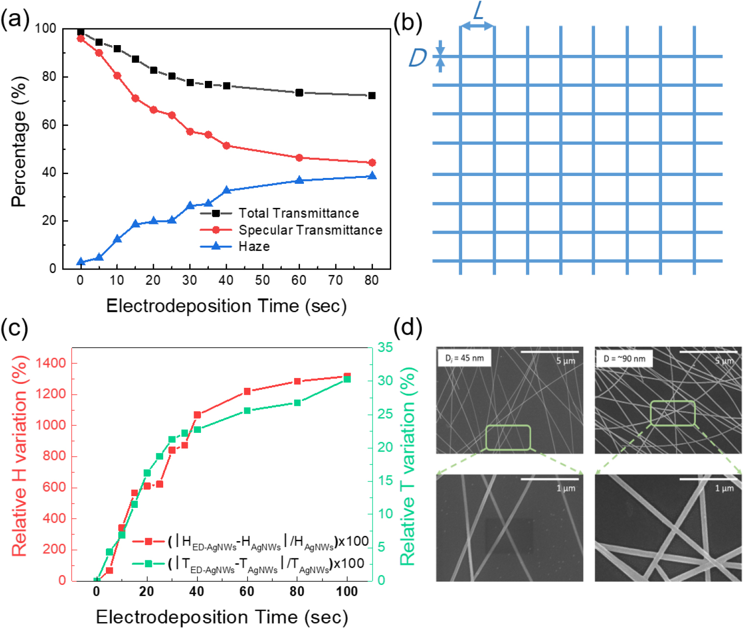
Fig. 2.
(a)Total transmittance, specular transmittance, and haze of the ED AgNW TCE for the light of wavelength 550 nm. (b) Square lattice structure for the nanonetwork with spacing L and diameter D. (c) Relative variation of the haze and the total transmittance for light of wavelength 550 nm after Ag electrodeposition. (d) SEM images of as-spin-coated (left) and ED-10 s (right) AgNWs network.
Based on the preceding discussion, the Rs can be decreased by extending the electrodeposition time. This reduction is attributed to the contributions from both the increase in wire diameter and the enhancement of wire-to-wire contact during electrodeposition. In the case where the Rs depends solely on the diameter of the AgNWs in the ED TCEs, it can be determined using the Eq. (7).25)
where, RED represents the Rs value after electrodeposition, Di stands for the diameter of the as-spin-coated AgNWs, DED refers to the diameter of the ED AgNWs, and Rspincoated denotes the Rs value of the as-spin-coated AgNW network. The experimental Rs values obtained for the AgNW network are significantly lower than the calculated RED values using the Eq. (7).25) The discrepancy observed between the measured Rs and the calculated RED is likely attributable to wire-to-wire welding facilitated by the electrodeposition of Ag at the junctions.
To rigorously evaluate the performance of ED AgNW TCEs across varying electrodeposition durations, the FoM is computed. The FoM, indicative of the effectiveness of the TCE, is defined as the ratio of the zero-frequency (DC) conductivity to the optical conductivity (σdc/σopt). Its calculation is expressed as Eq. (8).28)
where, T550 is Ttotal at 550 nm.
In this study, we have computed the FoM at a wavelength of 550 nm. Fig. 3(b) depicts the FoM values plotted against electrodeposition time. Remarkably, the calculated values of FoM for ED AgNW TCEs exhibit a consistent increase with prolonged electrodeposition durations. This observation indicates that the reduction in sheet resistance plays a predominant role in preserving the performance of ED AgNW TCEs.
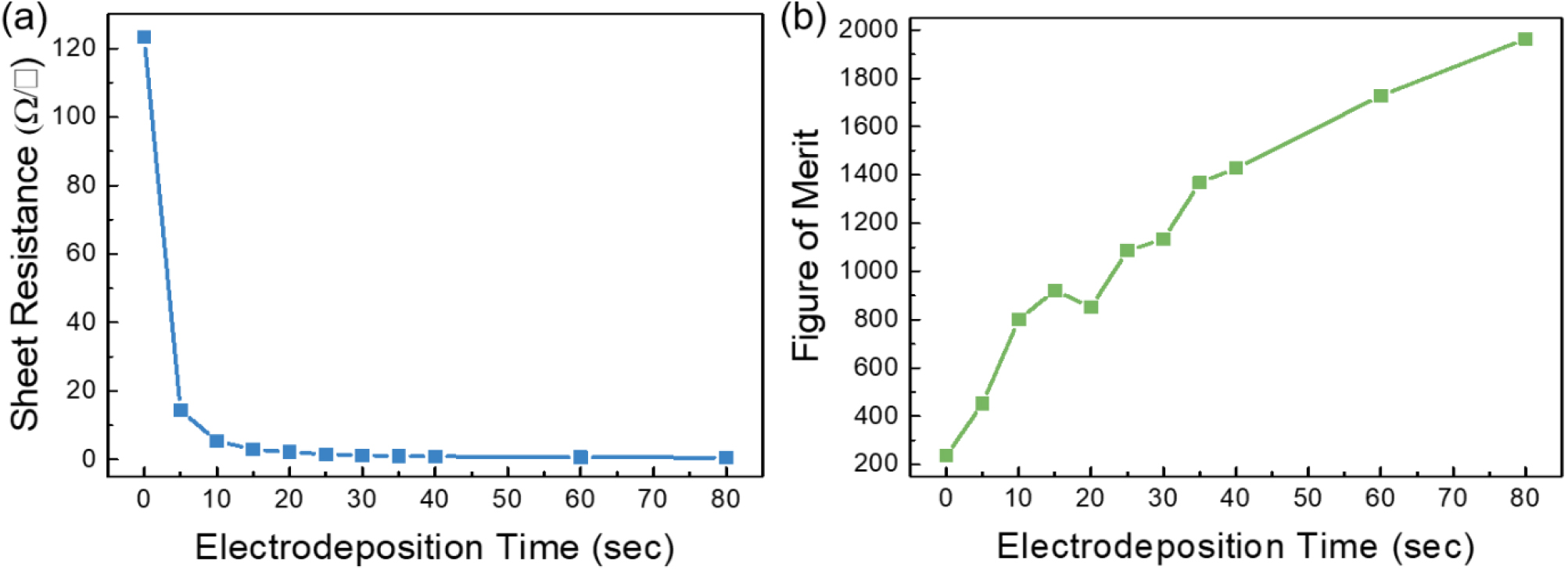
Relative changes in transmittance and haze occur rapidly within the first 40 s of electrodeposition. A similar trend is observed for both Rs and FoM. These observations provide valuable insights into optimizing electrodeposition time to improve the performance of the TCE. Based on this analysis, we selected a deposition time from this initial ramping region for the application in the CIGS solar cell. The J-V characteristics of CIGS solar cells utilizing ED AgNW TCEs were examined in comparison to those employing as-spin-coated TCEs.29,30)Fig. 4 illustrates the device performances through a comparison of their respective J-V characteristics. Notably, the performances of the devices utilizing ED AgNW TCEs were found to closely resemble those employing as-spin-coated TCEs. This similarity in performance suggests that cells featuring ED AgNW TCEs exhibit a performance level equivalent to that of cells utilizing as-spin-coated TCEs.
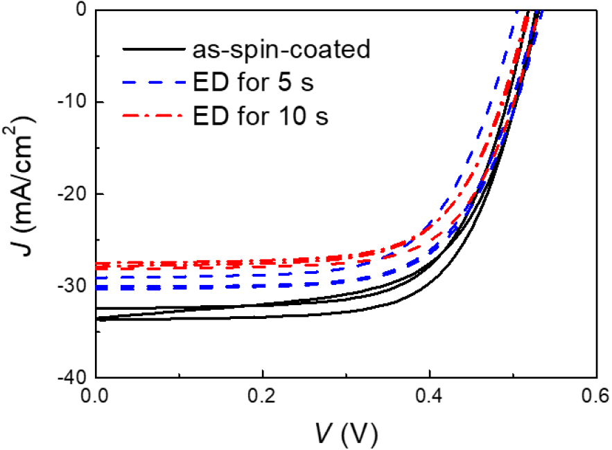
Performance metrics such as open circuit voltage (VOC), short circuit current density (JSC), efficiency, and fill factor (FF) of CIGS thin film solar cells utilizing both as-spin-coated and ED AgNW TCEs were derived from the J-V data and are consolidated in Table 1.
Table 1.
Open circuit voltage (VOC), short circuit current density (JSC), efficiency, and fill factor (FF) of CIGS thin film solar cells with as-spin-coated AgNW TCE, Ag ED for 5 s and 10 s AgNW TCEs.
The average power conversion efficiency was measured at 11.34 % for cells employing as-spin-coated TCEs, whereas for those utilizing ED TCEs, efficiencies were recorded at 10.19 % for 5-s electrodeposition duration and 9.66 % for 10-s electrodeposition duration. Moreover, the fill factors (FFs) across all cells were observed to be nearly indistinguishable.
4. Conclusion
We have effectively demonstrated and compared the optical and electrical characteristics of ED AgNW TCEs with those of as-spin-coated TCEs. Despite a minor decrease in T associated with increasing electrodeposition time, a significant reduction in Rs more than compensates for this effect, ultimately enhancing overall performance, as corroborated by the FoM. Upon integration of the ED TCE into CIGS solar cells and subsequent comparison with cells featuring as-spin-coated TCEs, similar performance levels were observed. The enhanced stability conferred by the electrodeposition process renders ED TCEs robust, advantageous, and reliable for a myriad of optoelectronic applications, without compromising performance.
