

1. Introduction
2. Experimental Procedure
2.1. Materials
2.2. Synthesis of Cu NWs
2.3. Synthesis of bimetallic Cu-Au nanostructures
2.4. Characterization
3. Results and Discussion
3.1. Characterization of bimetallic Cu-Au NTs and Cu@Au NWs
3.2. Electrical conductivity and thermal stability
4. Conclusion
1. Introduction
The structural and morphological control of nanostructures plays a pivotal role in tailoring their physical and chemical properties for a wide range of applications, including electronics, energy storage, and catalysis.1,2,3) Among various nanomaterials, one-dimensional (1D) Cu nanowires (NWs) have gained significant attention due to their excellent electrical conductivity, low cost, and compatibility with scalable synthesis methods.4) Additionally, the networking between NWs with high aspect ratios facilitates charge transfer along their longitudinal direction, leading to enhanced electrical conductivity. Cu is particularly attractive as a material, being 1,000 times more abundant and 100 times cheaper than Ag.5) These unique properties make Cu NWs promising candidates for use in flexible and transparent conductive electrodes, printed electronics, and thermal management devices.6) Precise morphological engineering of Cu-based nanostructures can be achieved through galvanic replacement and physical deposition. Galvanic replacement, a redox-driven process based on the differences in standard reduction potentials, enables the transformation of Cu NWs into hollow bimetallic nanotubes (NTs).7) On the other hand, physical deposition facilitates the formation of solid core-shell structures by directly coating Cu NWs with noble metals such as Au and Pt, offering a more controlled and dense morphology.8) Each of these methods offers unique advantages, such as structural tunability in galvanic replacement and enhanced protection in physical deposition.
Despite their attractive properties, Cu NWs face a major limitation: their high susceptibility to oxidation under ambient conditions. The rapid formation of copper oxides drastically increases junction resistance between NWs, leading to a marked rise in sheet resistance, which severely limits the performance of Cu NWs, particularly in applications requiring thermal or environmental durability.9) To mitigate these challenges, various surface modification strategies have been explored. Organic coatings, such as polymeric layers or self-assembled monolayers, offer some degree of antioxidation protection but lack long-term thermal and mechanical stability and exhibit poor electrical conductivity.10) Alternatively, carbon coatings, including graphene and amorphous carbon layers, provide better antioxidation performance. However, these coatings often introduce parasitic resistance or require complex processing, which compromises the conductivity and scalability of the Cu NWs.
To address these limitations, the physical deposition of Au onto Cu NWs can be effective since Au is chemically inert with high oxidation resistance, making it an ideal coating material for ensuring long-term stability without significantly compromising electrical conductivity.11) The resulting Cu@Au core-shell NWs are expected to combine the high electrical conductivity and low cost of Cu with the superior antioxidation properties of Au, offering a synergistic solution to the oxidation issue. Compared to galvanic replacement, physical deposition enables the formation of uniform Au shells without structural voids or significant Cu dissolution, thereby preserving the electrical performance and structural integrity of Cu NWs. In this study, we present the synthesis and characterization of Cu@Au core-shell NWs and compare them with Cu-Au NTs prepared via galvanic replacement. Our results demonstrate that Cu@Au NWs exhibit superior electrical conductivity (4 Ω sq-1) and exceptional thermal stability, maintaining their performance even after prolonged exposure to elevated temperatures (120 °C) and ambient air. These findings highlight the advantages of our physical deposition approach for producing durable, high-performance electrodes, making Cu@Au NWs a promising candidate for sustainable electronic and energy applications.
2. Experimental Procedure
2.1. Materials
The chemicals used in this study included copper (II) chloride dihydrate (CuCl2∙2H2O, ≥ 99.0 %, Sigma Aldrich), hexadecylamine (HDA, 98 %, Sigma Aldrich), dextrose (C6H12O6, Sigma Aldrich), gold (III) chloride trihydrate (HAuCl4∙3H2O, ≥ 99.9 %, Sigma Aldrich), L-ascorbic acid (C6H8O6, Sigma Aldrich), sodium hydroxide (NaOH, 93 %, Duksan Reagents), and polyvinylpyrrolidone (PVP, Mw = 55,000 g/mol, Sigma Aldrich), ethylene glycol (EG, 99.5 %, Duksan Reagents), and ethanol (EtOH, ≥ 99.0 %, Sigma Aldrich). Deionized (DI) water was obtained using an 18-MQ system (SHRO-plus DI).
2.2. Synthesis of Cu NWs
Cu NWs were synthesized using a hydrothermal method. First, 0.2418 g of CuCl2∙2H2O and 1.6545 g of HDA were dissolved in 70 mL of DI water with magnetic stirring at about 25 °C for 1 h. Subsequently, 0.5409 g of dextrose was added to the solution, which was then heated to 40 °C in an oil bath while stirring for 3 h. The resulting solution was transferred to a Teflon-lined stainless-steel autoclave and placed in a furnace for a hydrothermal reaction. The reaction was conducted at 120 °C for 16 h with a heating rate of 5 °C/min. After the reaction, the autoclave was allowed to cool naturally to about 25 °C. The Cu NWs were collected by centrifugation at 4,500 rpm for 8 min and washed three times with DI water and ethanol to remove residual impurities.
2.3. Synthesis of bimetallic Cu-Au nanostructures
The as-synthesized Cu NWs were redispersed in EG solution (60 mL) and equally divided into three beakers. Each of the three Cu suspensions was used for specific synthesis steps, with one suspension designated for the preparation of Cu-Au NTs and another for Cu@Au core-shell NWs. Separately, two EG solutions (2 mL each) containing 0.0112 g of HAuCl4∙3H2O were prepared. Then, Cu-Au NTs were synthesized via a galvanic replacement reaction between Cu2+ and Au3+. One of the EG solutions containing HAuCl4∙3H2O was added dropwise to one of the Cu suspensions containing PVP (0.05 g) at a controlled rate of 0.2 mL/min at about 25 °C. The reaction was allowed to proceed for 20 min. After the reaction, the products were collected by centrifugation at 7,500 rpm for 8 min. The Cu@Au core-shell NWs were synthesized using a similar method to the Cu-Au NTs. However, during the initial stage of redispersing a separate Cu suspension in EG, 0.0831 g of L-ascorbic acid and 0.0095 g of NaOH were added to the mixture.
2.4. Characterization
The morphologies of Cu NWs, Cu-Au NTs, and Cu@Au core-shell NWs were investigated using a JSM-IT700HR (JEOL) scanning electron microscope (SEM). X-ray diffraction (XRD) analysis was performed by a Rigaku MiniFlex 600 instrument with Cu Kα radiation (λ = 0.1542 nm) to confirm the crystal structure. The structures of bimetallic Cu-Au nanostructures were investigated using transmission electron microscopies (TEM; HT 7700, Hitachi, Japan; Titan G2 ChemiSTEM, FEI Company, USA). Energy-dispersive X-ray spectroscopy (EDS) elemental mapping images were obtained using an EDS spectrometer attached to the TEM. The sheet resistances of the films were measured by a four-point probe method with a Semi Auto Resistance & Resistivity Meter (RS8-1G, DASOLENG Co., Korea).
3. Results and Discussion
3.1. Characterization of bimetallic Cu-Au NTs and Cu@Au NWs
The experimental procedure for the synthesis of Cu-Au NTs and Cu@Au core-shell NWs is illustrated in Fig. 1. The preparation of these bimetallic nanostructures involves two key steps: (i) hydrothermal synthesis of Cu NWs and (ii) galvanic replacement for Cu-Au NTs or physical deposition of Au onto Cu NWs for Cu@Au NWs. In the first step, an aqueous solution containing copper (II) chloride dihydrate, HDA, and dextrose was prepared and heated at 40 °C in an oil bath under magnetic stirring for 3 h. Subsequently, the solution was transferred into a Teflon-lined stainless-steel autoclave, heated to 120 °C and maintained in a furnace for 16 h. During the hydrothermal synthesis, the Cu precursor was reduced into Cu nanostructures using dextrose as a reducing agent. It has been demonstrated that HDA molecules selectively adsorb on the (100) planes of growing Cu nanocrystals, stabilizing these planes and directing anisotropic 1D growth through a self-seeded growth mechanism.12) Additionally, PVP also plays a critical role as a surfactant, preventing aggregation, stabilizing the nanostructures, and ensuring the formation of well-defined Cu NWs. To induce the formation of bimetallic Cu-Au nanomaterials with distinct structures, two different methods were employed: galvanic replacement to synthesize Cu-Au NTs and physical deposition to fabricate Cu@Au NWs.
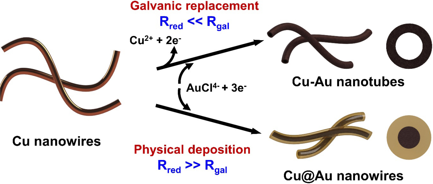
The Cu-Au NTs were achieved via a galvanic replacement reaction. The as-prepared Cu NWs were dispersed in an EG solution containing PVP as a surfactant, and the solution was mixed with another EG solution containing the Au precursor (HAuCl4∙3H2O) at a controlled rate of 0.2 mL/min. The reaction was carried out at room temperature under continuous stirring, during which [AuCl4-] ions were reduced by the sacrificial oxidation of copper (Cu0) atoms in the NWs. The newly formed Au atoms were directly deposited onto the surface of Cu NWs, loosely assembling into a porous structure. This redox process is governed by the difference in standard reduction potential between AuCl4-/Au0 (+0.99 V) and Cu2+/Cu0 (+0.34 V), favoring the replacement of Cu with Au.13,14) The galvanic replacement reaction is described by the following Eq. (1).
The electrons released from the oxidation of Cu atoms are consumed by [AuCl4-] ions, generating Au atoms that grow on the surface of the Cu NWs. As the reaction proceeds, Cu atoms within the NWs are continuously oxidized and dissolved, creating voids within the structure. Simultaneously, the deposition of Au atoms occurs preferentially at the Cu/Au interface, forming an Au shell around the original Cu core. This coupled process—simultaneous dissolution of the sacrificial metal (Cu) and deposition of the noble metal (Au)—is a key characteristic of galvanic replacement, which often leads to hollow or porous structures.15)
For the fabrication of Cu@Au NWs, the pre-synthesized Cu NWs were subjected to physical deposition of Au. This process involved dropping an EG solution containing the Au precursor into another EG solution containing the Cu NWs, L-ascorbic acid, NaOH, and PVP surfactants. The reaction was carried out under ambient conditions, during which the Au precursor was rapidly reduced and deposited onto the Cu NWs, forming a core-shell structure. The use of L-ascorbic acid facilitated fast reduction kinetics for Au3+ to Au0, favoring the immediate deposition of Au onto the Cu surface. This rapid reduction rate is significantly faster than the galvanic replacement reaction, where the deposition of Au atoms occurs at the expense of Cu oxidation. Furthermore, L-ascorbic acid was selected for its strong reducing capability, environmentally friendly nature, and scalability for practical applications, making it an ideal choice for this synthesis. As a result, physical deposition effectively minimizes Cu dissolution and oxidation, ensuring the formation of an Au shell that encapsulates the Cu core. In contrast to the slower galvanic replacement process, which promotes the formation of hollow or porous structures, the faster reduction kinetics in physical deposition favor the growth of solid core-shell morphology of Cu@Au NWs.
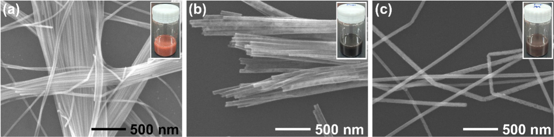
The overall morphologies and dimensions of the synthesized Cu NWs, Cu-Au NTs, and Cu@Au NWs were investigated using scanning electron microscopy (SEM) (Fig. 2). Fig. 2(a) shows a typical SEM image of Cu NWs with diameters and lengths ranging from 35 to 72 nm and 40 to 50 µm, respectively. The successful galvanic replacement and physical deposition were confirmed by the color changes in the colloidal suspensions, as depicted in the inset images of each panel in Fig. 2. The reddish color of Cu NWs transitioned to dark gray and dark brown for Cu-Au NTs and Cu@Au NWs, respectively. Fig. 2(b) clearly shows the hollow edges of the Cu-Au NTs. The morphological transformation of Cu NWs into Cu-Au NTs revealed two notable changes: an increased diameter (ranging from 60 to 110 nm) and a reduced length (~10 µm) compared to the starting Cu NWs. The increase in diameter is primarily attributed to the Kirkendall effect, a phenomenon arising from the unequal diffusion rates of Cu and Au atoms.16) During the reaction, Cu atoms diffuse outward to react with [AuCl4]-, forming Cu2+ ions that dissolve into the solution, while Au atoms deposit inwardly at a slower rate. This diffusion imbalance creates voids within the structure, leading to hollow interiors and outward structural expansion, which increases the diameter of the resulting Cu-Au NTs. In addition to the Kirkendall effect, the reduction in length is likely caused by stress-induced fragmentation during the alloying process.17) The formation of a Cu-Au alloy introduces significant lattice strain due to the mismatch in atomic sizes and lattice constants. This strain, combined with structural weakening from void formation, results in localized mechanical stress. These stresses are exacerbated by the hollow and porous nature of the intermediate structures, which act as weak points and make the NTs more prone to breaking. Unlike the Cu-Au NTs, Cu@Au NWs prepared by physical deposition exhibited a slightly increased diameter (ranging from 40 to 80 nm) and a slightly decreased length (10~30 µm) compared to the starting Cu NWs [Fig. 2(c)]. The slight increase in diameter is attributed to the deposition of an Au shell on the surface of the Cu NWs during the reduction of [AuCl4]- by L-ascorbic acid. The controlled deposition process, facilitated by fast reduction kinetics, ensures the formation of a continuous Au layer, leading to a marginal increase in the overall diameter. The slight decrease in length is likely due to stress-induced effects during the core-shell formation. The lattice mismatch between Cu and Au introduces minor strain at the interface, resulting in structural relaxation and a small contraction along the longitudinal axis of the NW. The chemical compositions of Cu-Au NTs and Cu@Au NWs were estimated to be Cu : Au = 0.74 : 0.26 and 0.69 : 0.31 in atomic fractions, respectively, through energy dispersive X-ray spectroscopy (EDS) measurements.
The detailed crystal structure of starting Cu NWs was investigated by XRD and TEM analysis (Fig. 3) Fig. 3(a) shows three characteristic diffraction peaks corresponding to the (111), (200), and (220) planes of Cu with a face-centered cubic phase (JCPDS# 04-836).18) Additionally, the absence of any peaks indicating secondary phases or Cu oxides confirms the high purity of the Cu NWs. Fig. 3(b) displays a typical TEM image of a Cu NW with a diameter of approximately 70 nm. It has been reported that Cu NWs grow from pentagonal Cu seeds with five-fold symmetry through a self-seeded growth mechanism.19) The clear lattice fringes in Fig. 3(c) and the corresponding selected area electron diffraction (SAED) pattern in Fig. 3(d) indicate that the NWs grow along the [110] direction. In particular, the SAED pattern clearly exhibits two superimposed zone axes, [001] and [12], of the face-centered cubic pattern. This observation suggests that the electron beam was aligned perpendicular to one of the five surfaces of the pentagonal cross-section of the five-fold twinned Cu NWs.20) Furthermore, Fig. 3(c) reveals that the twin planes are oriented parallel to the growth direction, confirming the multiple-twinned structure of the Cu NWs.
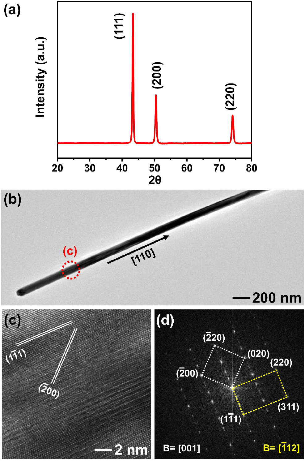
Fig. 3.
(a) X-ray diffractogram (XRD) of the as-synthesized Cu nanowires. (b) Low- and (c) high-magnification transmission electron microscopy (TEM) images of Cu nanowire [The red dot circle in panel (b) indicates the area of the high-magnification TEM image of (c)]. (d) Selective electron diffraction pattern (SAED) of Cu nanowire obtained from panel (c).
The distinct structures and elemental compositional distributions of both Cu-Au NTs and Cu@Au NWs were thoroughly investigated through TEM analysis. (Fig. 4) Low-magnification TEM images provide clear evidence of the hollow structure of the NTs, with an average diameter of ~100 nm [Fig. 4(a, b)]. The hollow morphology is a hallmark of the galvanic replacement reaction, which involves the outward diffusion of Cu and inward deposition of Au. Notably, the NTs are composed of fine alloy particles (< 5 nm), indicating that these particles loosely assemble into porous surfaces during the reaction. Elemental mapping images further confirm that Cu and Au are primarily concentrated on the walls of the NTs, with a uniform distribution observed along the tubular structure [Fig. 4(c, d)]. In contrast, the Cu@Au nanowire exhibits a solid core-shell structure, as clearly identified by the dark contrast of core regions in the TEM images [Fig. 4(e, f)]. The well-defined Au shell, formed during the physical deposition process, encapsulates the Cu core. Fig. 4(f) reveals that the shell is composed of Au nanoparticles, which are packed to form a shell layer. This observation is further supported by EDS mapping images [Fig. 4(g, h)], which distinctly show that elemental Cu is confined to the core region while Au is concentrated in the shell region. The clear separation of elemental distributions between the core and shell highlights the effectiveness of the deposition process in achieving a core-shell structure.
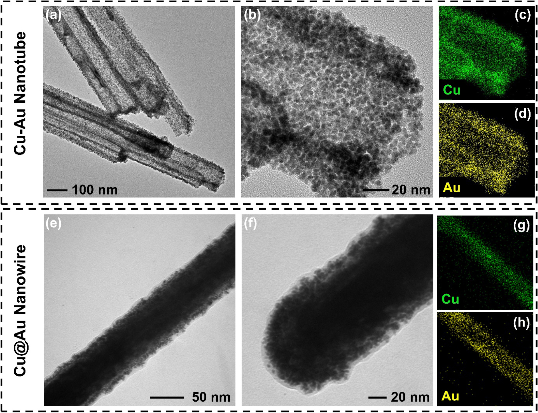
Fig. 4.
(a, b) Low-magnification transmission electron microscopy (TEM) images of Cu-Au nanotubes and (c, d) corresponding energy dispersive X-ray spectroscopy (EDS) mapping images of (c) Cu and (d) Au obtained from panel (b). (e, f) Low-magnification TEM images of Cu@Au nanowire and (g, h) EDS elemental mapping images of (g) Cu and (h) Au.
3.2. Electrical conductivity and thermal stability
To evaluate the electrical conductivity of the as-synthesized 1D nanostructures, we measured the sheet resistances of films consisting of Cu NWs, Cu-Au NTs, and Cu@Au NWs at approximately 25 °C. The films were prepared on a glass substrate by drop-casting suspensions of each sample, followed by heat treatment at 150 °C for 30 min in a mixed gas of 4 % H2 and 96 % Ar. Without annealing under reducing conditions, Cu NW films are known to be insulating due to residual surfactants and poor nanowire junctions.21) The measured sheet resistances of Cu NWs, Cu-Au NTs, and Cu@Au NWs were about 1, 10, and 4 Ω sq-1, respectively, indicating good conductivity and minimal variation after the transformation of Cu NWs into bimetallic Cu-Au 1D nanostructures [Fig. 5(a)]. These values represent the averages obtained from measurements taken at 10 different points on the sample. The slight increase in the sheet resistance of Cu-Au NTs is mainly attributed to their shortened length and hollow structure, which act as the scattering centers for charge transfer.
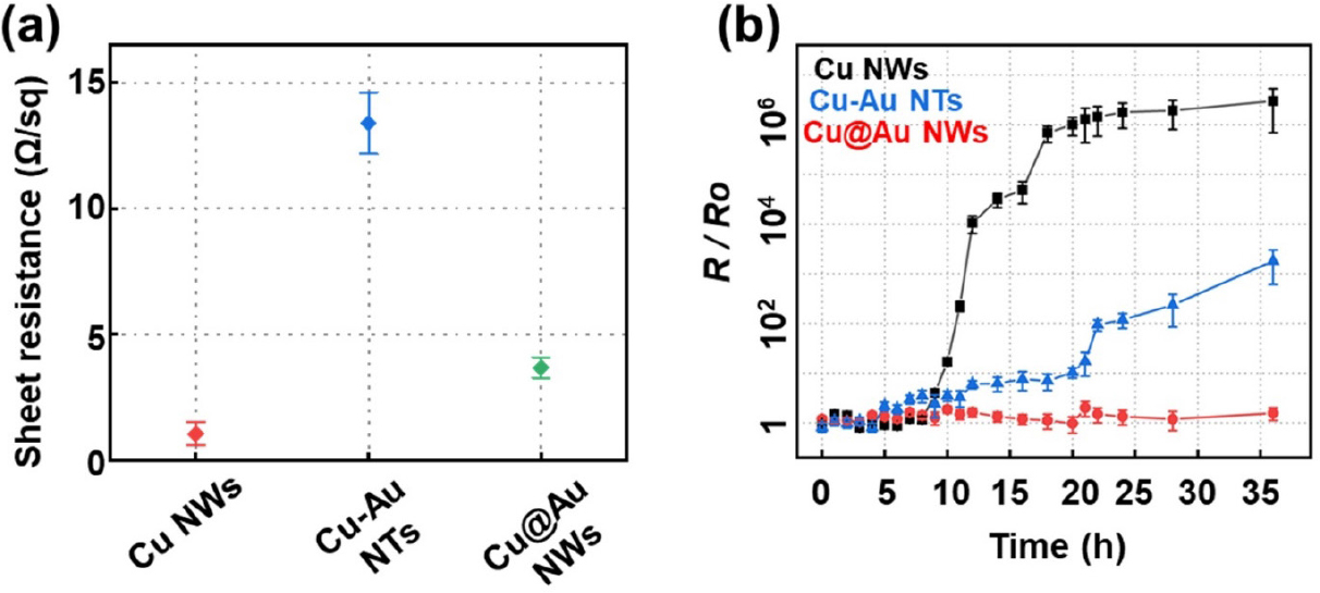
Long-term stability is crucial for the practical application of sustainable electrodes. However, Cu NWs are highly susceptible to oxidation under ambient conditions, which significantly increases the junction resistance between NWs, consequently raising the sheet resistance.22) Addressing this challenge, our physical coating approach, where Cu NWs are encapsulated with an Au shell, effectively mitigates oxidation while maintaining electrical performance. To investigate the thermal stability of the three samples, the variation of sheet resistances was monitored during storage at 120 °C under ambient air conditions. As shown in Fig. 5(b), the Cu NWs films exhibited a dramatic increase in sheet resistance, reaching 100 times the initial value within 10 h and 106 times after 20 h. In contrast, the Cu@Au core-shell NWs demonstrated exceptional stability, with the relative resistance (R/Ro) remaining almost constant (~1.36) even after 36 h. This superior stability is attributed to the chemical inertness of Au, arising from the lack of interaction between the orbitals of adsorbates and the filled d states of Au.23,24) Additionally, the high formation enthalpy of Au oxides (19.3 kJ/mol) further emphasizes the resistance of Au to oxidation.25) Meanwhile, the Cu-Au NTs showed a gradual increase in relative sheet resistance, with R/Ro reaching approximately 10 times the initial value after 22 h of storage. This instability, compared to the Cu@Au NWs, is primarily due to the shortened length of the NTs and insufficient passivation, which exposes Cu within their porous and hollow structure to oxidative degradation in aerobic environments. Therefore, our approach of physical deposition not only effectively prevents oxidation but also preserves low junction resistance, ensuring superior electrical performance. Moreover, the inherent chemical stability and high conductivity of the Au shell further enhance the long-term stability of the Cu@Au NWs, making this approach highly advantageous for applications requiring durable, low-resistance electrodes. These include flexible and transparent conductive electrodes for wearable electronics, foldable displays, and energy storage systems. Furthermore, the Cu-Au NTs with their porous structure and high surface area, are particularly beneficial for catalytic systems such as fuel cells and electrochemical sensors.
4. Conclusion
In this study, we successfully synthesized bimetallic Cu-Au NTs and Cu@Au core-shell NWs through two distinct methods: galvanic replacement and physical deposition. The structural and compositional analyses demonstrated that both processes effectively transformed Cu NWs into bimetallic 1D nanostructures, each exhibiting unique morphologies and properties. The galvanic replacement reaction yielded hollow Cu-Au NTs, driven by the outward diffusion of Cu and inward deposition of Au, a process governed by the Kirkendall effect. However, the resulting NTs exhibited increased sheet resistance and reduced thermal stability due to their shortened lengths, hollow interiors, and incomplete passivation of exposed Cu. In contrast, the physical deposition of Au onto Cu NWs produced Cu@Au core-shell NWs with a conformal Au shell, which effectively encapsulated the Cu core. This approach not only maintained the structural integrity of the Cu NWs but also minimized oxidation and dissolution, ensuring superior electrical performance and stability. The electrical conductivity and thermal stability tests further highlighted the advantages of the Cu@Au NWs. Compared to Cu-Au NTs and pristine Cu NWs, Cu@Au NWs exhibited the lowest sheet resistance (4 Ω sq-1) and exceptional thermal stability under harsh conditions (120 °C in ambient air), with minimal resistance variation (R/Ro ~1.36) even after 36 h. The remarkable stability can be attributed to the chemical inertness and high oxidation resistance of the Au shell, which effectively prevents the oxidation of the underlying Cu core. Overall, the Cu@Au core-shell NWs, with their enhanced thermal stability and durability, hold significant promise for use in sustainable and high-performance electrode applications.
