

1. Introduction
V-VI compound semiconductors have been studied for thin-film solar cell applications.1) Among them, the antimony selenide (Sb2Se3) thin film solar cell has reached 9.2 % efficiency.2) This material exhibits acceptable optical properties;3,4) Sb2Se3 has a bandgap of ~ 1.1 - ~ 1.3 eV and an absorption coefficient of ~ 105, which is comparable to those of Cu(InGa)Se2 (CIGS) and Cu2ZnSnS4 (CZTS). Therefore, Sb2Se3 is a promising alternative for the new thin-film solar cell applications.
Although 9.2 % Sb2Se3 devices have been achieved using vacuum processes,2) non-vacuum methods have an advantage in terms of low-cost production. Among them, electrodeposition is considered the best alternative method. It is possible to fabricate large-area, low-cost and eco-friendly solar cells compare to that of fabricated using vacuum methods. Many studies have examined thin film solar cells via electrodeposition, some of which have reported good device performance.6,7) Nevertheless, few studies have investigated Sb2Se3 solar cells using electrodeposition. Y. Kwon et al. reported a Sb2Se3 thin film solar cell with an efficiency of 1.8 % using this method,8) but further study will be necessary to improve the conversion efficiency. Recently, many researches using non-toxic materials for solar cells applications are in progress. Among them, Sb2Se3 solar cell is also included. However, high efficiency Sb2Se3 solar cell using wet process is not reported yet.
In this study, Sb2Se3 thin films were fabricated by electrodeposition, and the photovoltaic properties of Sb2Se3 thin film solar cells were investigated. The electrodeposition conditions to form Sb2Se3 thin films were optimized. The orientation of the resulting Sb2Se3 thin films annealed at various temperatures from 230 to 310 °C was then analyzed. Finally, the photovoltaic properties of the resulting Sb2Se3 thin-film solar cells were examined.
2. Experimental Procedure
2.1. Thin-film preparation
The electrolytes consisted of 1 mM antimony potassium tartrate [K2Sb2(C4H2O6), Sigma-Aldrich Inc., St. Louis, MO, USA], 2 mM selenous acid (H2SeO3, Sigma-Aldrich Inc., St. Louis, MO, USA), and 400 mM potassium chloride (KCl). The pH of the solution was fixed to 2.00 ± 0.01 using hydrochloric acid (HCl). Cyclic voltammetry (CV) and electrodeposition of the Sb2Se3 thin films were performed in a three-electrode system using a potentiostat (PARSTAT 2273, Princeton Applied Research). This three-electrode system contained soda-lime glass (SLG) substrates coated with fluorine doped tin oxide (FTO, 3 × 3 cm2), Pt mesh, and Ag/AgCl (in 1 M KCl) as the working, counter, and reference electrodes, respectively. The FTO was cleaned ultrasonically in the order of acetone, ethanol, and distilled water for 10 min, and dried with N2 gas. CV was performed on a unitary Sb, Se system, and a binary Sb-Se system, respectively. The scan rate was fixed to 50 mV/s and the negative direction was first measured. Electrodeposition was performed from -0.5 V to -0.8 V based on Ag/AgCl (in 1 M KCl). After electrodeposition, annealing was carried out from 230 °C to 310 °C for 20 min in an N2 atmosphere. The heating rate was 10 °C/min.
2.2. Solar cell fabrication
After annealing, a 50 nm CdS buffer layer was deposited via chemical bath deposition. Subsequently, an intrinsic 50 nm ZnO (i-ZnO) layer and a 350 nm transparent Al-doped ZnO (AZO) conducting layer were deposited by radio frequency (RF) and direct current (DC) magnetron sputtering, respectively. A Ni-Al electrode was deposited via electron beam evaporation. The Sb2Se3 solar cell structure was composed of SLG/FTO/Sb2Se3/ CdS/i-ZnO/AZO/Ni-Al.
2.3. Characterization
The morphology and composition of the films were observed by field-emission scanning electron microscopy (FE-SEM, TESCAN MIRA 3) with an energy disperse X-ray spectroscope (EDS). The structural characteristics of the films were analyzed by X-ray diffraction (XRD, Rigaku Ultima IV). The solar cell parameters were analyzed by current density-voltage (J-V) measurements with a designated area of 0.522 cm2 (under standard AM 1.5 illumination).
3. Results and Discussions
3.1. Electrochemical behavior
The electrochemical behavior of Sb and Se was investigated by CV. Fig. 1 shows cyclic voltammograms indicating the electrochemical behavior of the Sb, Se, and Sb-Se system. Regarding the electrochemical behavior of Sb (red), tartaric acid increases the solubility of Sb, where Sb is present in water in the form of SbO+. The reduction peak was observed at -0.59 V; this was attributed to the reduction of SbO+ to Sb on FTO glass,9-11) and is expressed by the following chemical reaction:
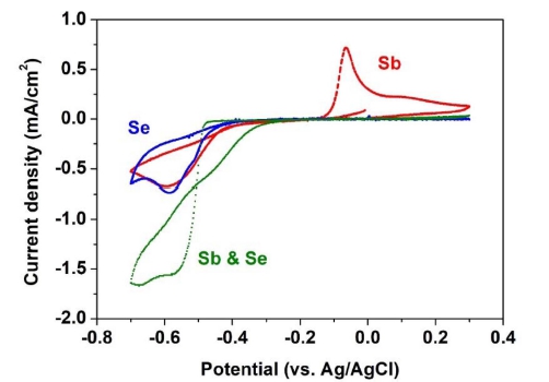
Fig. 1
Cyclic voltammograms of FTO glass in Sb solution (1 mM K2Sb2(C4H2O6) + 400 mM KCl), Se solution (2 mM H2SeO3 + 400 mM KCl), and Sb-Se solution (1 mM K2Sb2(C4H2O6) + 2 mM H2SeO3 + 400 mM KCl).
The blue-colored cyclic voltammogram indicates the electrochemical behavior of the Se system. The reduction peaks were observed at -0.51 V and -0.58 V. According to previous studies,12,13) the first peak at -0.51 V was attributed to the deposition of bulk Se through a fourelectron reduction of H2SeO3 to Se. The reaction was

In addition, another peak at -0.58 V was attributed to the six-electron reduction of H2SeO3 to H2Se according to the following formula:14)

The product H2Se may undergo a comproportionation reaction when the H2SeO3 concentration is high enough.15) The comproportionation reaction is as follows:

Finally, regarding the electrochemical behavior of the Sb-Se system (green), reduction peaks were observed at -0.58 V and -0.67 V. The reduction peak at -0.58 V was attributed to the deposition of Sb and Se via the following reaction:16,17)
With a further negative potential, another peak at -0.67 V was also associated with the formation of Sb2Se3, but may also be synthesized via a different route as follows18)
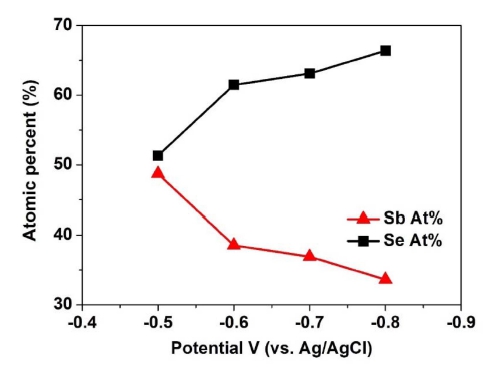
Based on the electrochemical behavior found by CV, Sb2Se3 thin film deposition was performed over the potential range of -0.5 V to -0.8 V, and Fig. 2 shows the composition ratio of Sb2Se3 thin films. As shown in Fig. 2, the Se contents increased gradually with increasing potential. In addition, the stoichiometric composition of the Sb2Se3 thin film was observed at -0.6 V. Therefore, the potential of -0.6 V was chosen for the electrodeposition of Sb2Se3 thin films.
3.2. Structural characterization
As shown in Fig. 3, XRD was used to determine the crystallinity of the thin films. Without annealing, an amorphous phase and only a peak corresponding to SnO2 were observed due to the poor crystallinity.19) After annealing, the thin film showed the Sb2Se3 phase with an orthorhombic structure. Theoretical calculations have indicated that the recombination loss could be reduced when Sb2Se3 grows on the c-axis [(211) and (221)], and the device performance increases with decreasing growth in the (120) direction.2) Therefore, the preferred orientation of the Sb2Se3 thin film was analyzed from the XRD peak intensity ratio. Fig. 4 presents the XRD peak intensity ratio showing the change in the orientation of the Sb2Se3 thin film with annealing temperature. At 230 °C, the XRD peak intensity ratio of (221)/(120) and (211)/(120) was 2.2 and 2.64, respectively. In the Sb2Se3 thin film annealed in the range of 230 ~ 310 °C, the largest XRD peak intensity ratio of (221)/(120) and (211)/(120) was observed at 250 °C, which were 2.93 and 3.3 respectively. At annealing temperatures higher than 250 °C, the XRD peak intensity ratio of (221)/(120) and (211)/(120) decreased gradually. This means that the Sb2Se3 thin film annealed at 250 °C grew most in the c-axis direction.
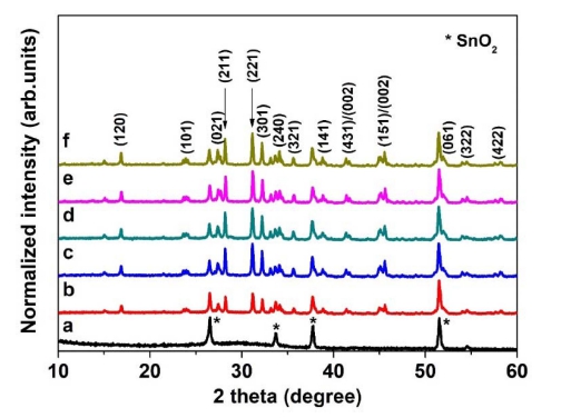
Fig. 3
XRD patterns of Sb2Se3 thin films annealed at different temperatures; (a) As-deposited, (b) 230 °C, (c) 250 °C, (d) 270 °C, (e) 290 °C, (f) 310 °C.
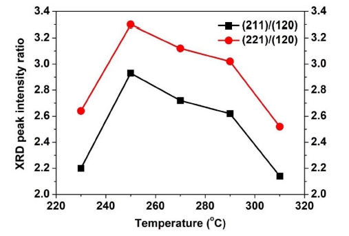
Fig. 4
XRD peak intensity ratio of (211)/(120) and (221)/(120) of Sb2Se3 thin films annealed at temperature in the range of 230 ~ 31 0°C.
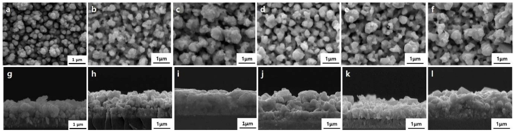
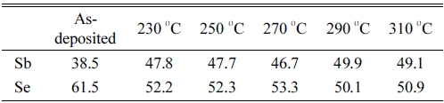
Fig. 5 presents FE-SEM images of Sb2Se3 thin films annealed in the range of 230 ~ 310 °C. In addition, a comparison of the as-deposited thin film and annealed thin-film revealed the surfaces of the annealed films to be rougher than the surfaces of the as-deposited films. Because Se has a high vapor pressure, the evaporation of Se appeared to have occurred with the annealing temperature was increased.20) Table 1 lists the composition of the annealed Sb2Se3 thin film at each annealing temperature. When annealing was carried out, Se loss occurred at all annealing temperature ranges. Although annealing was performed at a low vacuum (~5 × 10 kPa) and low temperature (230 ~ 310 °C), the Se loss have occurred.
3.3. Current density-voltage (J-V) analysis
Fig. 6 presents the J-V analysis results of Sb2Se3 thin film solar cells annealed in the range of 230 ~ 310 °C. Table 2 lists the photovoltaic performances obtained from these cells. Among the Sb2Se3 thin films annealed in the range of 230 ~ 310 °C, the Sb2Se3 cell annealed at 250 °C showed the highest conversion efficiency owing to the largely improved JSC compared to the other cells. The improved JSC was attributed to the enhanced orientation in the Sb2Se3 thin film. As shown in Fig. 4, relatively large growth in the c-axis direction, i.e., growth in the (211) and/or (221) directions, was observed in the Sb2Se3 thin film annealed at 250 °C. As the Sb2Se3 thin film grew in the c-axis direction, the [Sb4Se6]n nanoribbons became vertical to the substrate. This leads to the smooth movement of carriers, thereby increasing the carrier collection probability.2) On the other hand, other Sb2Se3 thin-film solar cells exhibited lower conversion efficiency due to poor JSC.
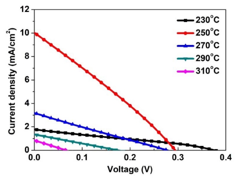
Fig. 6
J-V characteristics of Sb2Se3 thin film solar cells annealed at temperature in the range of 230 ~ 310 °C.
Table 2
Photovoltaic performance for Sb2Se3 thin film solar cells annealed at temperature in the range of 230 ~ 310 °C.
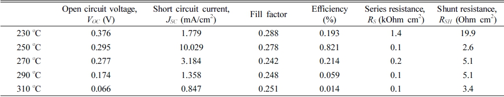 |
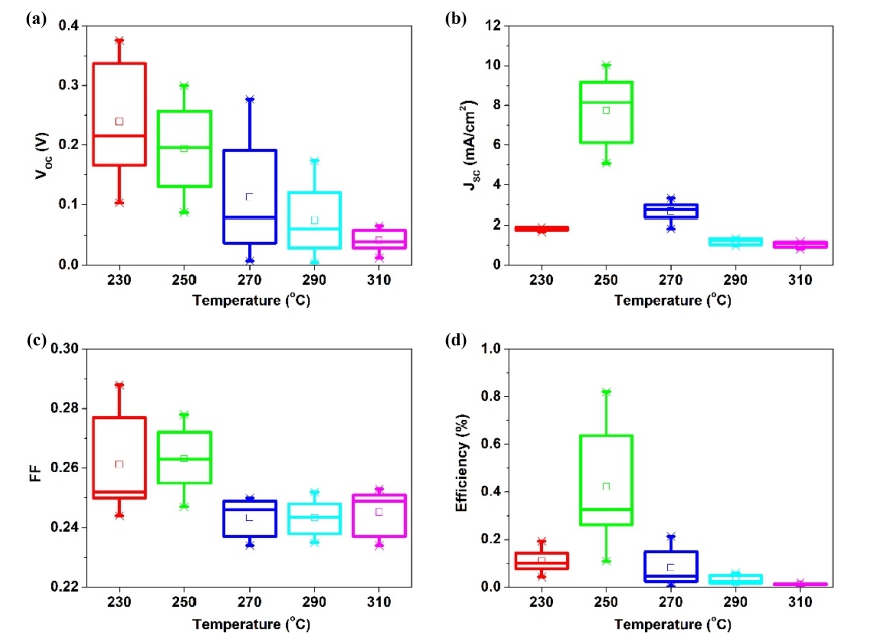
Although JSC was improved by modified orientation, most Sb2Se3 thin-film solar cells suffer lower conversion efficiency due to the poor VOC and FF. As shown in Fig. 7(a), the VOC is very low compared to other research examining the orientation of Sb2Se3.21) The decrease in VOC appears to be caused by interface recombination at CdS/Sb2Se3. As described in section 3.2, the surface roughness was higher than the as-deposited film because of the Se loss.22,23) This appears to harm CdS formation, which results in poor P-N junction quality. In addition, the FF was largely limited by parasitic resistance effects, as shown in Table 2. The rough surface condition is believed to be a possible reason for the small shunt resistance (RSH). Moreover, the large series resistance (RS) exhibited by Sb2Se3 annealed at 230 °C is related to the poor crystallinity of the thin film. On the other hand, the large value of RS in the other cells can be due to FTO/absorber interface.
4. Conclusions
This study examined a different approach to the fabrication of Sb2Se3 thin films. As deposited Sb2Se3 thin films were deposited by electrodeposition and annealed at temperatures in the range of 230 ~ 310 °C. The influence of the annealing temperature on the Sb2Se3 thin film and the resulting solar cell devices were examined. CV was performed to investigate the electrochemical behavior in the electrolyte. The results showed that the stoichiometric composition of Sb2Se3 appeared at -0.6 V. In addition, the orientation of the Sb2Se3 thin films was dependent on the annealing temperature. XRD showed that the Sb2Se3 thin films annealed at 250 °C grew most in the (211) and/or (221) orientation. The (211) and/or (211) direction growth led to the smooth movement of carriers, thereby increasing the carrier collection probability. Fig. 5 SEM data showed the enhanced performance when particles are homogeneous and have good crystallinity. Therefore, the solar cell using Sb2Se3 thin-film annealed at 250 °C exhibited significant enhancement in the JSC of 10.03 mA/cm2 and the highest conversion efficiency of 0.821 % because of the preferred orientation of the Sb2Se3 thin film.
