

1. Introduction
As the IT industry has expanded, there has been a significant increase in the number of semiconductor manufacturing plants and the related facilities and equipment. This growth has, in turn, driven a higher demand for high-purity tubes, which are essential for transporting the highly corrosive gases used in semiconductor production processes.1,2,3,4) Tubing and piping used in the semiconductor sector must maintain a high level of cleanliness, with stainless steel being the material of choice. STS316L is preferred due to its superior resistance to corrosion, a characteristic that comes from its chemical composition, which includes 10-14 % nickel and 16-18 % chromium, making it slightly more resistant than STS304L.5,6) Moreover, the thin oxide layer (passive film) made of CrO and FeO on the surface acts as a protective barrier, preventing the underlying metal from reacting with harmful elements such as moisture and oxygen.7)
Melting processes have been widely studied in the literature, with particular attention given to vacuum induction melting (VIM) and vacuum arc remelting (VAR).8,9,10) In the VIM process, high-purity gas is used to assess and enhance the quality and contamination levels of the final ingots. VIM aids in smoothing the surface and improving alloy uniformity, primarily due to the stirring effect created by the induction field and the precise control of the melt’s superheat.11,12,13,14) On the other hand, the VAR process is a secondary refining method used to homogenize materials with high melting points and sensitivity to oxygen, such as the seamless tubes employed in semiconductor manufacturing. In VAR, the material is melted under vacuum conditions, which helps eliminate impurities and reduce porosity in the ingots. When both VIM and VAR are combined, the process is often referred to as double melting (DM).15,16,17)
Electrolytic polishing (EP) is commonly applied in various industries such as semiconductor, medical, and ultra-clean gas applications. EP delivers excellent results when the polished inner surfaces of tubes and pipes come into contact with pure gases. The performance of semiconductor devices heavily depends on the purity of the gas flowing through the STS316L tubes. The inner surface of stainless steel must not only reduce surface roughness (Ra) but also enhance corrosion resistance by removing damaged layers and impurities that contribute to surface corrosion. Electrolytic polishing is regarded as one of the most effective techniques for achieving these goals.15,16,17,18,19)
Cl2 gas is used in semiconductor processes such as plasma etching and epitaxy. However, due to its highly corrosive nature, prolonged exposure to Cl2 gas can potentially lead to corrosion of the piping used in semiconductor processes.20) Previous studies have primarily reported the corrosion mechanisms of STS316L induced by Cl2 gas at high temperatures. However, research on corrosion mechanisms and surface properties within the temperature range typically encountered in semiconductor processes remains insufficient.21,22) Moreover, there is a lack of studies on how Cl2 exposure affects the stability of EPed DM-processed STS316L surface properties.
Therefore, the objective of this study is to investigate the changes in the characteristics of the electrolytic polished layer on DM-processed STS316L when exposed to Cl2 gas.
2. Experimental Procedure
In this study, STS316L samples produced by DM processes were used. These tubes were then subjected to electrolytic polishing. Electropolishing was performed on the inner surface of a 1/4” tube using an electrolyte solution composed of H3PO4, H2SO4, and DI water in a 6:3:1 volume ratio. The process conditions were set to 2.9 V, with a current density of 0.14 A/cm2, a polishing time of 300 s, and an electrolyte temperature of 60 °C. For the Cl2 gas exposure test, the electropolished tube was cut to a length of 10 cm using slow-speed cutting. The tubes were exposed to Cl2 gas for 1, 5, 9, and 13 d. During the exposure, Cl2 gas was introduced at a pressure of 76 kPa, and after 5 min, the valve was closed to maintain a pressure of 92 kPa. The internal temperature was kept between 34 °C and 42 °C, and the humidity inside was set to below 30 ppb. Upon retrieving the samples, high-purity nitrogen gas was used for purging the interior for 20 min. For surface characterization and microstructural observation, the electropolished tube was cut into 1 cm-long specimens and then longitudinally halved. Surface roughness was assessed using a surface profilometer. The thickness of the electrolytically polished layer was measured using Auger Electron Spectrometer (AES, PHI 700Xi) with a sputtering rate of 0.47 nm/min. The thickness was determined by multiplying the sputtering rate by the time required for the oxygen concentration to decrease to half of its maximum value. The ratios of Cr/Fe and CrO/FeO were calculated using the equation previously reported, based on data obtained from X-ray photoelectron spectroscopy (XPS, Thermo VG).23) Scanning electron microscope (SEM) and energy-dispersive X-ray spectroscopy (EDS) analyses were conducted to observe the microstructure and elemental distribution of the sample. The measurements were performed using a JSM-7800F (JEOL) at an accelerating voltage of 5.00 kV with a magnification of 1,000×. EDS mapping was subsequently performed on the same region to identify the distribution of Cr, Cl, Fe, and O (SEM-EDS, JSM-7800F, JEOL).
3. Results and Discussion
Fig. 1 presents the surface roughness results of the EP layers depending on the Cl2 exposure time, measured with a surface profiler. Surface roughness was evaluated using two standard parameters: Ra, the arithmetic average of surface height deviations from the mean line, and Rz, the average maximum peak-to-valley height over a sampling length. As the exposure duration increased to 0, 1, 5, and 9 d, the surface roughness showed significant changes. The Ra values were 0.01, 0.04, 0.04, and 0.03 µm, while the corresponding Rz values were 0.04, 0.20, 0.14, and 0.16 µm, respectively. Although these variations may appear numerically small, especially in the case of Ra, they indicate meaningful changes at the microscale surface level. The increase in Rz, in particular, suggests that localized surface damage or pitting may be progressing with exposure time, which reflects degradation of the initially smooth EP layer.
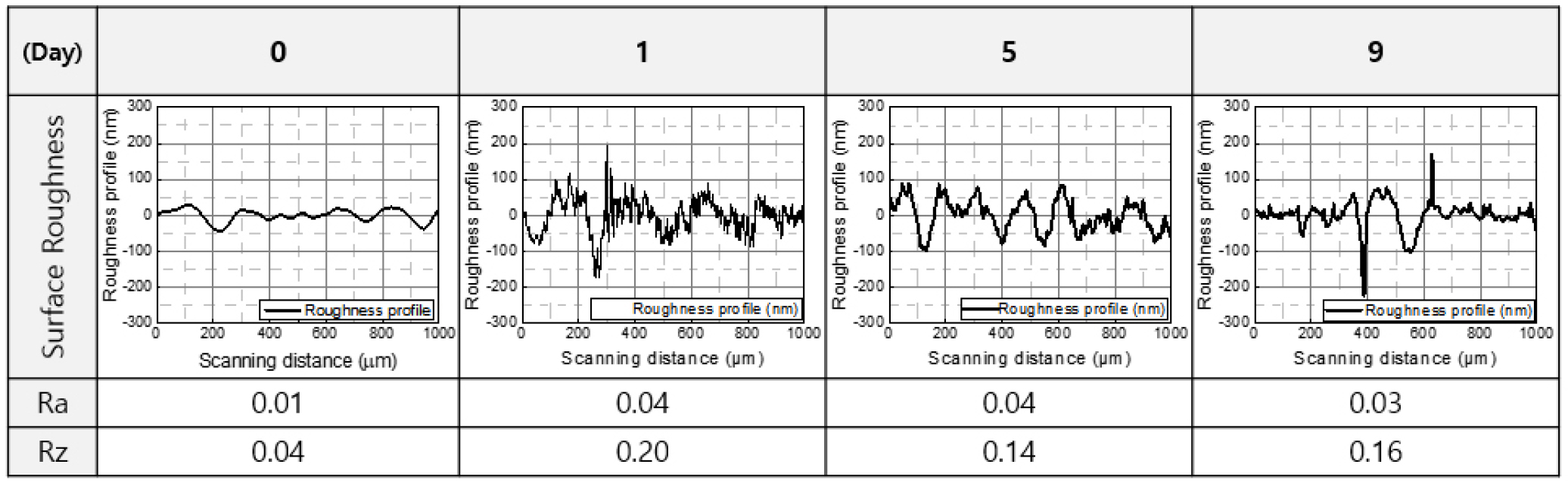
Fig. 2 showed the AES analysis results used to determine the oxide layer thickness. As the sputtering time increased, the signal intensities of Fe and Cr increased, while the intensity of oxides decreased. The oxide thickness was calculated by multiplying the sputtering rate by the time at which the oxygen signal dropped to half of its maximum intensity. The thickness of the EP layer on STS316L decreased to 8, 3.18, 2.58, 0.51 nm after 0, 1, 5 and 9 d of Cl2 gas exposure, respectively. From day 0 to day 9, the EP layer thickness steadily decreased, but after 9 d, no significant changes were observed. In the DM specimen without EP treatment, an oxide layer of 2.38 nm was observed, indicating that the initially formed EP layer had been fully removed by day 5.
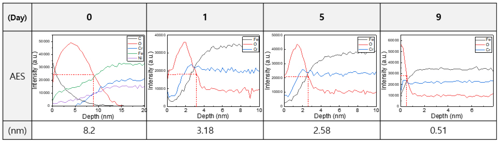
Fig. 3 presents a graph that illustrates the depth and distribution of Cl penetration in the specimens, depending on the duration of Cl2 exposure. The y-axis represents the Cl concentration at exposure times of 1, 5 and 9 d, while the x-axis shows the corresponding depths of Cl penetration. It is evident that the depth of penetration increases over time, with the depth corresponding to the precise thickness of the EP layer, excluding the base material.
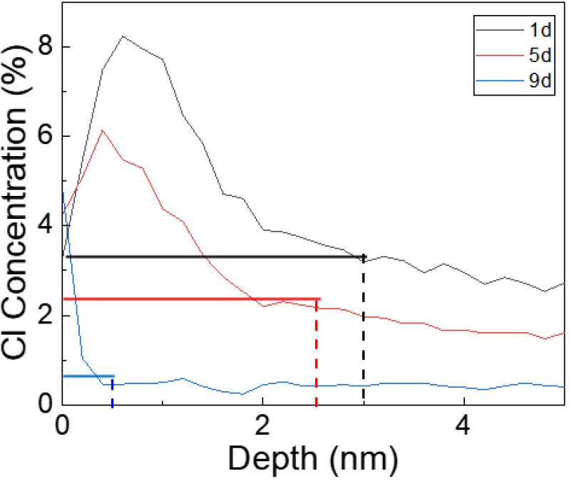
Fig. 4 shows the concentration profiles of Cl and Cr were analyzed using AES, revealing a clear inverse correlation between the two elements. In regions where the Cl concentration increased, a noticeable decrease in Cr concentration was observed. This suggests that Cl penetrates the EP layer and either damages or replaces the Cr-rich oxide layer. Since both Cl and Cr concentrations are presented in relative atomic percentages, a higher relative presence of Cl at the surface corresponds to a lower relative concentration of Cr. These results indicate that prolonged exposure to Cl2 gas may gradually degrade the protective Cr2O3 layer within the surface oxide, thereby reducing corrosion resistance.
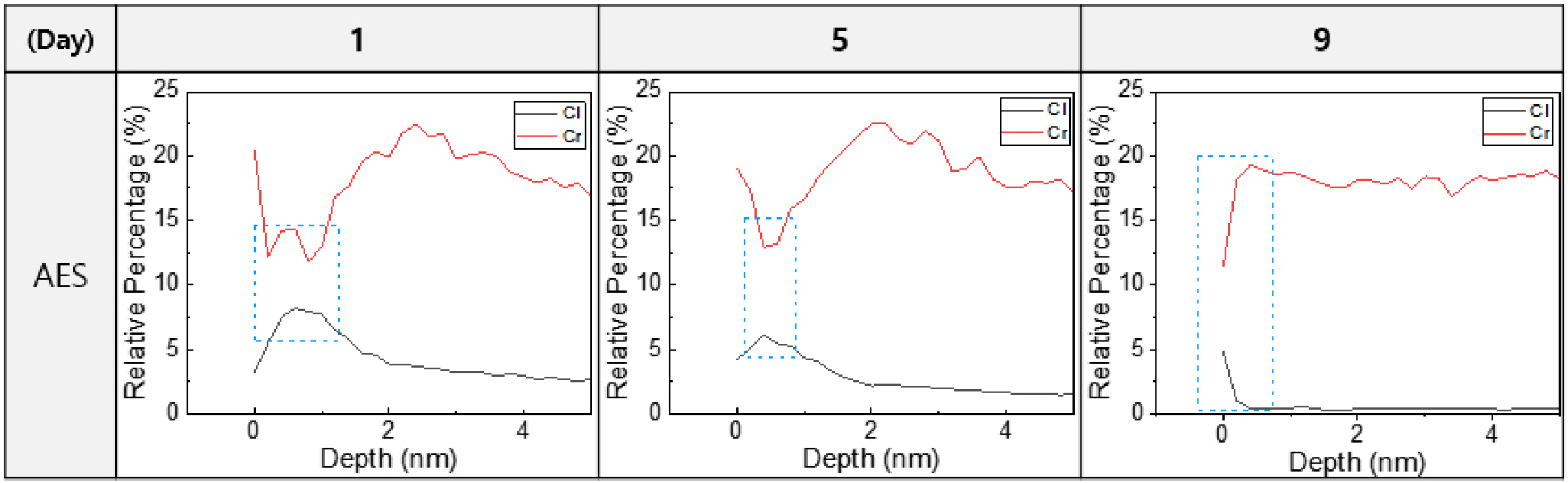
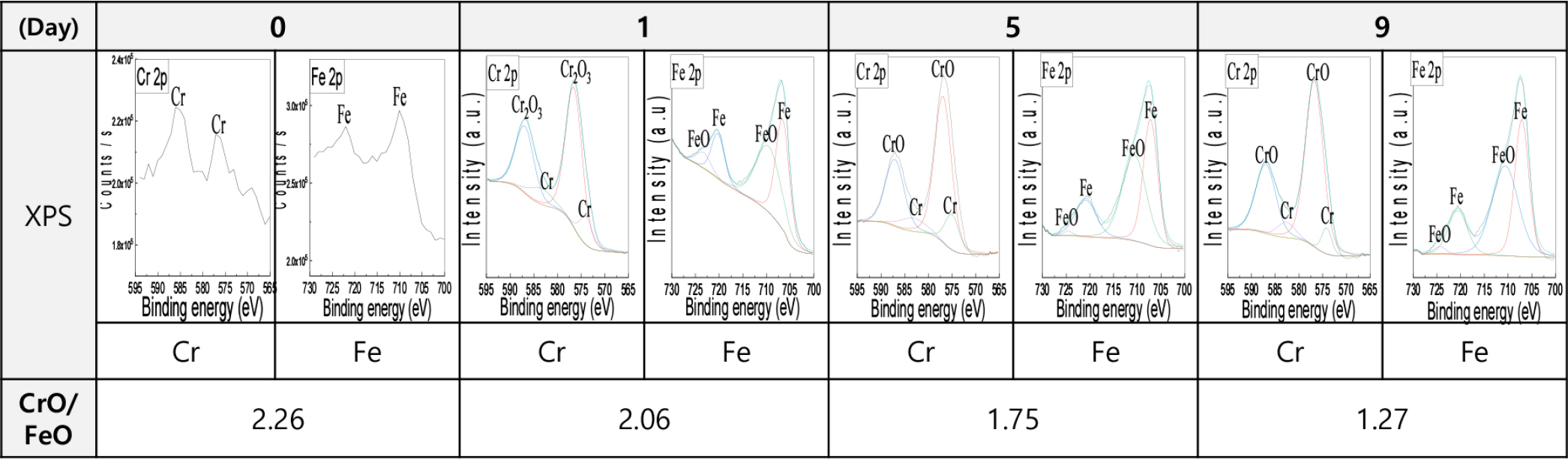
Fig. 5 presents the XPS analysis results for the EP layer of STS316L after Cl2 exposure for 1, 5 and 9 d. Prior to Cl exposure, the CrO/FeO ratio was 2.26. After exposure for 1, 5 and 9 d, the ratios were 2.06, 1.75 and 1.27, respectively. Similar to the AES results, the CrO/FeO ratio decreased continuously from day 0 to day 9, after which no significant changes were observed.
Standard reduction potentials, as summarized in Bratsch24) help explain the corrosion mechanism by indicating the thermodynamic tendency of redox reactions. Chlorine gas acts as a very strong oxidizing agent, capable of oxidizing both chromium and iron. In Table 1,25) if the value obtained by subtracting the anode potential from the cathode potential is greater than zero, a reaction can occur. The larger this value, the more reactive the substance is. Therefore, since the value of chromium minus chlorine is greater than that of iron minus chlorine, it can be concluded that chromium reacts more readily with chlorine than iron does.
The corrosion mechanism of the STS316L substrate in Cl2 gas environments involves chlorine penetrating through defects or cracks in the passivated layer, as reported in previous studies. Upon penetration, chlorine reacts with metal elements at the metal layer interface, forming metal chlorides. Metal chlorides then undergo redox reactions, transforming into Cr2O3 and Fe2O3. However, metal oxides do not provide the protective effect similar to the passivated layer. This cycle repeats, eventually leading to the corrosion of STS316L through Cl2 gas.25)
Fig. 6(a) shows an SEM image of pitting corrosion observed on a specimen of STS316L after exposure to Cl2 gas for 1 d, and (b) is the corresponding EDS image. In the SEM image, pitting corrosion is observed, and the EDS map reveals that both Cr and Cl are present in the same area, while Fe is absent. This suggests that chromium chloride may have formed on the surface layer.
Consequently, to evaluate the stability of the EP layer on DM STS316L under a highly corrosive environment simulating semiconductor processes, specimens were exposed to Cl2 gas for up to 9 d. As the exposure duration increased, surface roughness gradually increased, while the oxide layer thickness and the CrO/FeO ratio decreased, indicating gradual degradation of the protective Cr2O3 film.
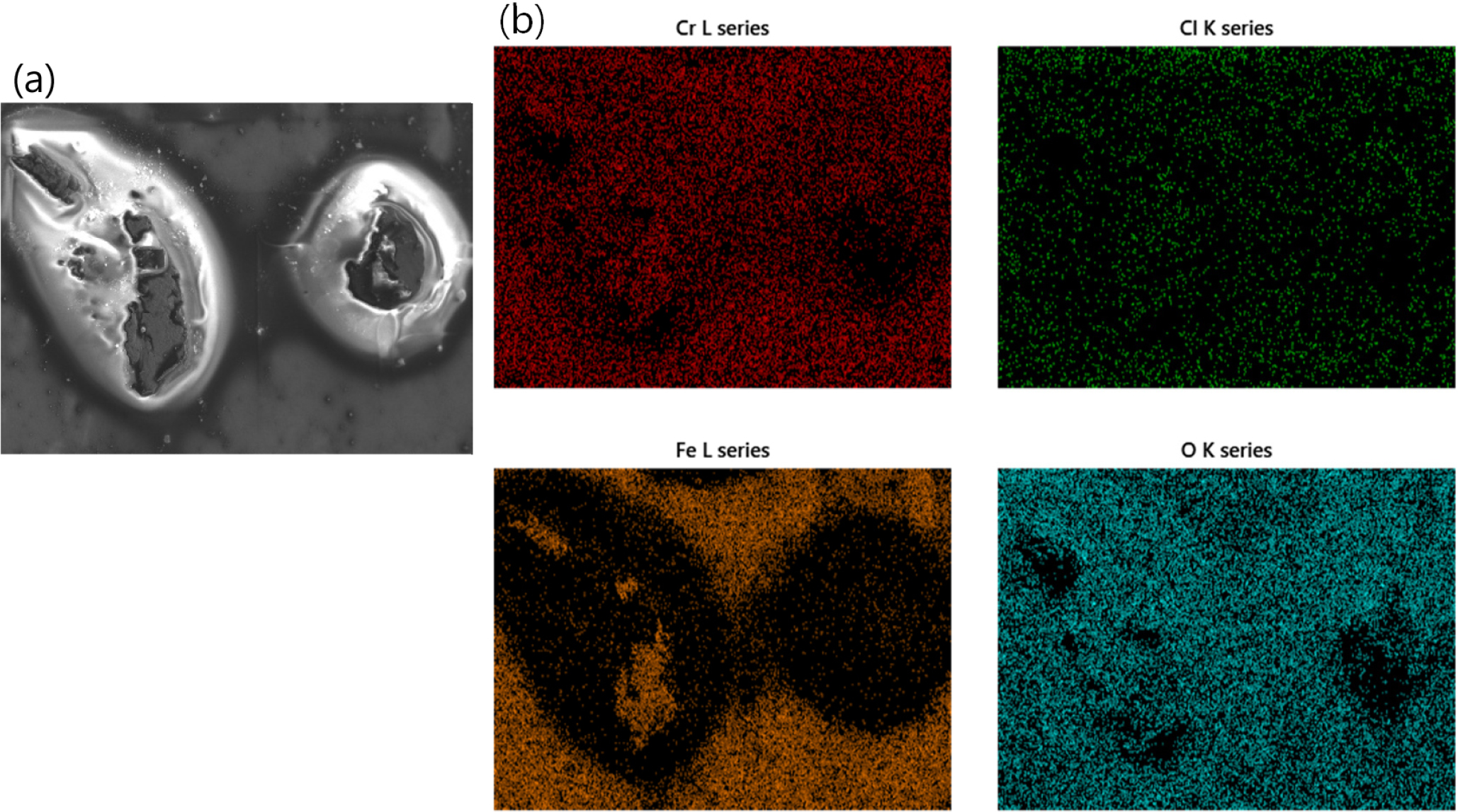
Table 1.
Standard reduction potentials at 298 K.25)
| Element | Reaction | E0 (volts) |
| Chlorine | Cl2(g)+2e- ⇌ 2Cl- | 1.360 |
| Chromium | Cr3+ + 3e- ⇌ Cr(s) | -0.74 |
| Cr2+ + 2e- ⇌ Cr(s) | -0.89 | |
| Iron | Fe2+ + 2e- ⇌ Fe(s) | -0.44 |
4. Conclusion
The tubes were exposed to Cl2 gas, commonly used in semiconductor processes, for durations ranging from 1 to 9 d. Surface roughness, measured with an alpha-step profilometer, showed significant changes with values of 0.01, 0.04, 0.04 and 0.03 µm for exposure times of 0, 1, 5 and 9 d, respectively. The oxide layer on STS316L measured 2.38 nm before EP and increased to 8.2 nm after EP. Upon Cl2 exposure from 1 to 9 d, the oxide thickness decreased from 3.18 nm to 2.58 nm and 0.51 nm. No significant change was observed thereafter, indicating near-complete removal of the EP layer by day 5. Additionally, XPS analysis revealed that the CrO/FeO ratio decreased from 2.06 after 1 d of exposure to 1.27 after 9 d, indicating a reduction over time. Similarly, no significant change was observed beyond day 9. These results demonstrate that Cl2 exposure significantly impacts both the surface roughness and chemical composition of the material, with the CrO/FeO ratio decreasing and the EP layer becoming thinner as exposure time increases. These findings suggest that prolonged exposure to Cl2 may compromise the corrosion resistance of STS316L and contribute to the initiation of pitting corrosion. From the standpoint of semiconductor equipment and materials, it may be beneficial to explore additional protective coatings, optimized alloy designs, or the use of more corrosion-resistant materials such as Hastelloy, depending on the operating conditions.
