

1. Introduction
Dye-sensitized solar cells(DSSCs) have the advantage of low-cost and large scale fabrication on flexible substrates. 1-3) However, the energy conversion efficiency(ECE) of perovskite solar cell is about 20 %, and that of DSSC is relatively low at about 11 %, requiring further research into solve this problem and achieve commercialization.4)
The improvement in the ECE of the DSSC involves studying all its components, including the working electrode(WE), electrolyte, and counter electrode(CE). In particular, the greatest focus has been on improving the WE. In the case of the WE, the dye plays a role forming electrons and holes upon absorbing light, and the electrons and holes are respectively transferred to the WE and CE. There has been a recent increase in the study of dye regarding electron mobility or the amount of light absorption.
First, in order to increase electron mobility, the thickness of the semiconductor oxide layer(mesoporous TiO2) needs to be controlled or the band gap should be changed. J. Dewalque et al.5) reported that an existing ECE of 2.9 % increased to 5.8 % by changing the thickness of the semiconductor oxide layer from 0.9 to 4.0 μm due to the increased absorption of the amount of dye. E. Palomares et al.6) reported that the existing ECE of 3.8 % increased to 5.0 % by reducing the recombination due to coating the Al2O3 having a larger band gap on mesoporous TiO2.
Second, in order to increase the amount of light absorption, the specific surface area of the semiconductor oxide layer needs to increase or a new material should be employed. Y. Noh et al.7) reported that the existing ECE of 4.66 % increased to 5.25 % applying polystyrene beads of a thermoplastic polymer into the TiO2 layer to increase the specific surface area while forming pores. H. Koo et al.8) reported that the existing ECE of 7.79 % increased to 9.43 % with an increase in the amount of dye absorbed due to the presence of a hollow structure TiO2 layer. N. Yao et al.9) reported that the existing ECE of 1.3 % increased to 4.48 % as a result of the conversion of light form visible into the UV range by employing a phosphor of ZnO : Eu3+, Dy3+.
In particular, a recent study of localized surface plasmon resonance(LSPR), which employs a nano-metal powder into the semiconductor oxide layer, was carried out to increase the amount of light that is absorbed. LSPR is such that free electrons vibrate due to a resonance between the wave and the precious metal electrons according to the incoming light. The LSPR effect can create strong near-field electromagnetic fields and far-field propagating waves, which could then be used to enhance the light absorption.10) H. Jung et al.11) reported on an increase in ECE to 4.34 %, which is an enhancement by 11 % when compared with the existing 3.89 % after adding 0.07 wt% Au nano particles into the mesoporous TiO2 layer due to the increase in the amount of light absorbed with LSPR.
However, in the case where Au nano particles are added into the TiO2 layer, there is difficulty in going through the complicated process of synthesizing Au nano particles. The Au particles formed agglomerates that lead to a reduction in the shunt resistance. Also, when Au nano particles are employed into the TiO2 layer, there is difficulty in uniform dispersion as well as in keeping the electron transport path due to the reduction in the fraction of the TiO2 path for a large amount of Au particles.
In this study, we coated the Au nano-thin films with thicknesses of 0.0, 0.5, 1.0, and 5.0 nm by using sputtering on the TiO2 blocking layer(BL) to confirm the LSPR induced an improvement in ECE.
2. Experimental Details
In this study, we prepared DSSC devices with Au thin film coating with a thickness of 0.0 to 5.0 nm on the TiO2 BL. We produced 300 nm-thick BLs by mixing titanium(IV)bis(ethyl aceto acetato)-diisopropoxide and 1- butanol into a solution, followed by spin-coating for 500 rpm-10 sec. and 2000 rpm-40 sec., and then heat treating at 500 °C for 15 min.
The Au thin films were prepared via ion sputtering (JFC-1500, JEOL) to form Au layers with a thickness of 0.0 to 5.0 nm on BL using 99.99 % Au as a target at room temperature.
We analyzed the surface microstructure of the BL with the Au thin films via field emission scanning electron microscopy(FE-SEM, S-4300, Hitachi) at an acceleration voltage of 15 kV. Here, the samples have a structure consisting of glass/FTO/BL/Au layer that were prepared via heat treatment at 500 °C for 30 min., which is the same as heat treating temperature for the TiO2 layer.
Also, the increase in the specific areas of the BL resulting from coating with Au thin flims was determined by scanning an area of 3 × 3 μm2 with an atomic force microscope(AFM, SPM25DRM, Park Scientific Instruments) in the non-contact mode, and the surface roughness was determined by measuring the root mean square(RMS). Here, samples with a structure consisting of glass/FTO/ BL/Au layers were prepared via heat treatment at 500 °C for 30 min., which is the same as the heat-treating temperature of the TiO2 layer.
We fabricated 8 μm-thick TiO2 films by coating the TiO2 paste with a particle size of 20 nm(DSL 18NR-T of 10, Dyesol) via a doctor blade method and via heat treatment at 500 °C for 30 min.
The LSPR phenomenon of the TiO2 layer with the Au thin flims was assessed by conducting an analysis through a micro-Raman spectrometer(UniRaman Model, Unithink). At this time, the characteristic peaks were checked in the range from 100 to 250 cm−1 by conducting scans for 60 times with an exposure value of 1 sec. using an accumulation mode with a center value of 600 cm−1 for each sample.
We adsorbed 0.5 mM cis-vis bis-ruthenium (II) bistetrabutylammonium( N719) on TiO2 and completed the WE consisting of glass/FTO/BL/Au nano thin film/TiO2/ dye(N719).
The absorbance of the WE that was prepared was analyzed via UV-VIS-NIR(UV3105PC, Shimadzu) with an absorption-mode apparatus under a medium scan speed. The average absorbance in the visible-light region of 400 to 800 nm was obtained by adding the absorbances at each wavelength and dividing this figure by the number of times of the addition.
The CE was prepared via RF sputtering(MHS-1500, Moohan, 300W, 13.56 MHz) to form a 100 nm-Pt film on a glass substrate using 99.99 % Pt as a target. A flow of 40 sccm Ar at a pressure of 5 mtorr at RT was set for the process, and the prepared WE and CE were fixed at the position and were filled with electrolyte, finalizing the DSSC device consisting of glass/FTO/BL/Au thin film/ TiO2/dye(N719)/electrolyte/100 nm Pt/glass with an active area of 0.45 cm2.
The impedance of the DSSC was determined using a solar simulator(PEC-L11, Peccell) and a potentiostat (Iviumstat, Ivium) in order to verify the interfacial resistance. The analysis was carried out in the frequency range from 10 mHz to 1 MHz by applying an AC voltage and collecting the current responses. The I-V(currentvoltage) characteristics of the DSSC were measured using the same instruments under a setup with a 100 W Xenon lamp as the illumination source under a 1 sun(100 mW/ cm2) condition. From the I-V curves, the short-circuit current density(Jsc), the open-circuit voltage(Voc), the fill factor(FF), and the ECE were evaluated.
3. Results and Discussion
Fig. 1 shows FE-SEM images of the BL on FTO substrates employing Au films with thicknesses of (a) 0.0, (b) 0.5, (c) 1.0, and (d) 5.0 nm after heat treatment at 500 °C for 30 min.
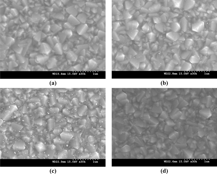
Fig. 1.
FE-SEM images of the blocking layers with Au layers ; (a) 0.0 nm, (b) 0.5 nm, (c) 1.0 nm, and (d) 5.0 nm.
Fig. 1(a) shows that the FTO with a particle size of 500 nm could be confirmed and that the BL was conformally coated on the entire surface of the FTO. Fig. 1(b) shows uniform coating of the Au film on the FTO, as shown in Fig. 1(a). This confirms that spherical particles with a particle size of 30 nm at a density different of 5.64 ea/μm2 were generated. This result was due to the rapid diffusion that occurred even through the heat treatment of 500 °C, 30 min., which could be available only in nano-thick films. Fig. 1(c) shows that spherical particles with a particle size of 50 nm had been generated at a density different 12 ea/μm2 on the FTO substrate. Meanwhile, Fig. 1(d) shows a uniform coated layer along the FTO substrate without forming agglomerates after heat treatment at 500 °C for 30 min. In this case, the expectation was that improving the ECE by increasing the electron recombination and decreasing the electron transport at the TiO2 layer would be disadvantageous.
Therefore, the LSPR phenomenon was expected by forming agglomerates even with a low heat treatment at 500 °C by coating the Au thin film at certain nano thickness on the BL.
Fig. 2 shows the root mean square(RMS) results of the BL employing Au films with thicknesses of (a) 0.0, (b) 0.5, (c) 1.0, and (d) 5.0 nm on flat glass substrates with heat treatment at a temperature of 500 °C for 30 min. The RMS values were determined using an AFM image in the upper left inset.
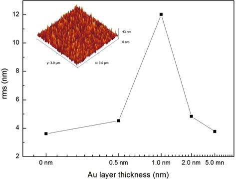
The RMS values of the BLs with 0.0, 0.5, and 1.0 nm Au thin films were 3.61, 4.53, and 12.01 nm, respectively, so we verified the increase in the specific surface area of the BLs by employing Au thin films compared to that of bare BL. In particular, the RMS value increased as the Au thickness increased until 1.0 nm. This result was due to the rapid diffusion of the low-temperature heat treatment for a nano-thick Au films, as discussed earlier in the FE-SEM results. Meanwhile, in the case of the Au thin film of 5.0 nm, the RMS value decreased rapidly to 3.7 nm.
This was due to the insufficient thermal energy from the low-temperature heat treatment to form agglomerates, as already shown in the FE-SEM results.
Fig. 3 shows micro-Raman data of the WE samples with a structure of glass/FTO/BL/0.0~5.0 nm-thick Au thin film/ TiO2.
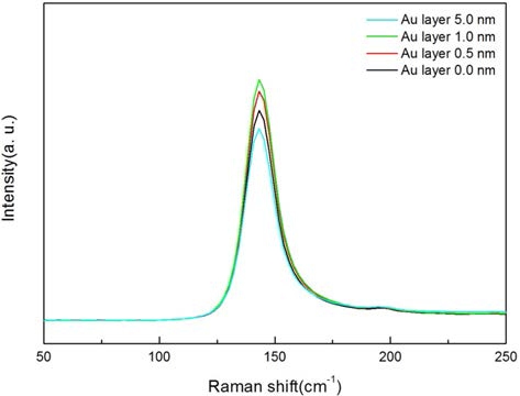
All of the TiO2 layers with and without the Au thin films showed a Raman characteristic peak of 144 cm−1, as reported by J. Xu et al12) reported. Also, the intensity in the Raman characteristic peak at 144 cm−1 gradually increased as Au film thickness increased. This is the result of the increase in the absolute amounts of incident light due to the LSPR phenomenon. Meanwhile, the intensity of the Raman characteristic peak decreased for the 5.0 nm Au thin film. This result indicates that the LSPR effect may disappear at this thickness condition.
Therefore, our results imply that an Au thin film with proper thickness induced the LSPR phenomenon by forming nano agglomerates.
Fig. 4 shows the Nyquist diagram consisting of real number and imaginary number for the frequency applied to the DSSC device with a structure consisting of glass/ FTO/BL/0.0~5.0 nm-thick Au thin film/TiO2/dye(N719)/ electrolyte/100 nm Pt/glass. Parts for each resistance Rh, R1, R2, R3 are also displayed in the upper left inset.
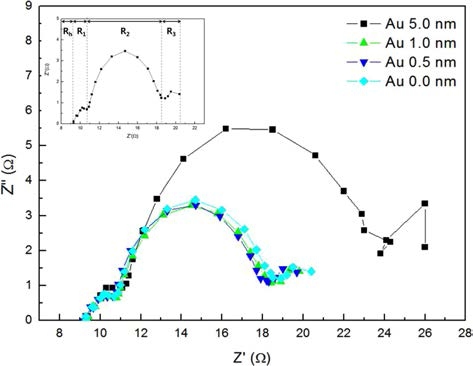
The R1 value at 103~105 Hz represents the interfacial resistance of TCO/TiO2 and electrolyte/CE, and it was shown to be identical at about 1.45 Ω for all devices. This was considered as the result produced by use of the same Pt CE and electrolyte.
The R2 value represents the factor showing the resistance to the electron movement in TiO2 and the TiO2/ electrolyte interface resistance at 1-103 Hz, and it is shown to be 8.2 Ω, 7.7 Ω, and 7.6 Ω upon the deposition of 0.0, 0.5, and 1.0 nm of Au thin film, respectively. As shown in the micro-Raman result, the decrease in the R2 values was due to the LSPR effect that was considered to be the result of an increase in the electron generation. However, in the case of the 5.0 nm Au thin film, the R2 value was confirmed to be 13.2 Ω, which was considered to be the result caused by acting as a new electrode layer with uniform deposition and an increase in the electron recombination.
The R3 value corresponds to the Warburg impedance related to the diffusion of oxidation-reduction species in the electrolyte at frequencies higher than 106 Hz, and it was measured to be about 1.5 Ω in all cases within the range of error, which was considered to be the result produced by the use of the same electrolyte.
Thus, we have confirmed that the deposition of the proper thickness of Au thin film on the BL increased in light absorption and generated electrons by the LSPR effect, reducing the electron transport resistance.
Fig. 5 shows the I-V data for the DSSC device with a structure consisting of glass/FTO/BL/0.0~5.0 nm-thick Au thin film/TiO2/dye(N719)/electrolyte/100 nm Pt/glass.
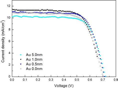
Fig. 5.
I-V characteristics of the DSSCs employing the Au layers of 0.0~5.0 nm (light intensity: 100 mW / cm2, AM 1.5 G filter).
The Voc were observed within the error range, while the Jsc and FF could be confirmed to have increased upon deposition of more than 1.0 nm after a decrease of up to 1.0 nm. When the appropriate thickness of the Au thin film was employed, the Jsc and FF could be improved due to the increase in the LSPR effect, as shown in the results of the Raman spectroscopy.
Table 1 shows detailed photovoltaic data from the I-V curves of Fig. 5.
Table 1.
Photovoltaic performance and energy conversion efficiency of DSSC.
| Au layer thickness(nm) | Voc(V) | FF | Jsc(mA/cm2) | η(%) |
|---|---|---|---|---|
| 0.0 | 0.70 | 0.65 | 10.93 | 5.15 |
| 0.5 | 0.71 | 0.67 | 11.04 | 5.28 |
| 1.0 | 0.70 | 0.69 | 11.39 | 5.34 |
| 5.0 | 0.71 | 0.67 | 10.30 | 4.98 |
Voc showed similar values of 0.70 V within the error range, and the similar values of Voc were considered to be attributable to the use of the same electrolyte in all fermi levels as an element related to the oxidationreduction reaction of the electrolyte.
In the case of FF, the value of 0.65 was observed in the device without the deposition of the Au thin film. Otherwise, 0.67 and 0.69 were confirmed in the case of 0.5 and 1.0 nm, respectively. As shown in the micro- Raman results, an increase in FF was due to the LSPR effect, which was considered to be the result of an increase in the electron generation. In the case of the 5.0 nm Au film, the value of FF was confirmed to be 0.67, which was considered to be a result of the insufficient thermal energy to form agglomerates.
The Jsc was 10.93 mA/cm2 in the device without deposition of the Au thin film while values of 11.04 mA/ cm2 and 11.39 mA/cm2 were observed in the case of the 0.5 nm and 1.0 nm thin films, respectively. The Jsc increased with an increase in the thickness of the Au thin film, and this was the result of the LSPR effects forming Au agglomerates, and the light absorption increased. In the case of the 5.0 nm Au film, the value of Jsc was confirmed to be 10.30 mA/cm2, which indicated that the Au films acted as a new electrode layer to increase the electron recombination.
In the case of the ECE, it was observed to have increased to 5.15, 5.28, and 5.34 % upon Au thin films with a thickness of 0.0, 0.5, and 1.0 nm, respectively. This was the result of the increase in Jsc and FF according to the LSPR effects. In the case of the 5.0 nm Au film, the value of the ECE was confirmed to be of 4.98 %, which was considered to be the result caused by decrease in Jsc and FF.
Therefore, we successfully proposed DSSC devices with an improvement in ECE due to LSPR effects by depositing an Au thin film of a proper thickness on the BL.
4. Conclusions
We employed Au films with thicknesses of 0.0 to 5.0 nm on the BLs of DSSCs. In the case of heat treatment at a temperature of 500 °C, the Au agglomerates with a particle size of less than 50 nm formed on the BL and the intensity of the Raman characteristic peaks for TiO2 were confirmed to have increased due to the LSPR effects with Au thin films of certain thickness. The photovoltaic results showed that the ECE became 5.15 % with the 1.0 nm thick-Au thin film. This improvement was a result of the increase in the LSPR of the TiO2 layer resulting from coating the Au thin film. Thus, by employing the appropriate thickness of the Au thin film, we have demonstrated an improvement in the ECE of DSSC.
