

1. Introduction
To utilize the extraordinary properties of graphene, such as its unique electronic transport, excellent thermal conductivity, and high mechanical strength in numerous potential applications,1-3) various growth methods have been devised including mechanical or chemical exfoliation as well as direct growth on SiC or metal substrates.3-9) Specifically, the chemical vapor deposition (CVD) of graphene on transition metals such as Ni, Cu, Pd, and Pt has enabled the growth of high-quality graphene layers over large areas and its implementation into a variety of applications.6-9) However, in this method, a feasible graphene transfer process from metals to desired substrates is required for the realization of graphenebased applications, and the development of a perfect transfer technique that causes no damage and contamination to pristine graphene remains a great challenge.
Currently, the most common transfer methods are based on the complete etching of metal substrates in suitable etchants with a polymer supporting layer such as poly(methyl methacrylate) (PMMA) or polydimethylsiloxane during the etching process.10,11) However, this wet etching transfer process is not suitable for applications of large-scale graphene films, as it leads to inevitable damage to the graphene and unintentional contamination or metal particle residue on the graphene layer. In addition, this chemical etching method not only imposes a high material cost during large-scale production because it dissolves the expensive high-purity metal catalysts, but it also requires long treatment cycles, such as etching and cleaning processes, which exceed several hours.11)
Recently, Gao et al. suggested a facile transfer technique based on the mechanical separation of graphene from a Pt foil using H2 bubbles generated from the cathode of an electrolytic cell.12) This bubbling transfer method requires tens of seconds only and is nonconstructive, not only to the graphene but also to the metal substrates, which allows for the repeated growth of graphene. To date, however, there are no detailed studies of the H2 bubbling-assisted transfer of graphene grown on a Cu foil, the most commonly used catalystic substrate material for growing graphene in the CVD process. Here, we report an H2 bubbling-assisted transfer technique on a Cu foil and demonstrate the origin of the graphene tearing phenomenon induced by this transfer process. Furthermore, we introduce an improved H2 bubbling transfer method for graphene grown by CVD on Cu foils using two hot metal plates pressed against each other with precisely controlled temperature and pressure levels.
2. Experimental Procedure
Using a hot-wall CVD, graphene was grown on 25-μm thick Cu foils (Alfa Aesar, item No. 13382). All the gas flow rates were controlled by mass flow meters calibrated by N2 in units of sccm. A typical growth process is as follows: a piece of Cu foil cut into 5 cm × 5 cm was loaded into a fused silica reaction tube, then evacuated to 1 × 10⁻³ Torr; the foil was annealed at 1,000 °C for 30 min in an H2 ambient atmosphere (H2 flow rate of 5 sccm) to remove the native oxide layer and contaminations on a Cu foil and to smooth the Cu surface; graphene growth was initiated by introducing 10 sccm of CH4 for 30 min at a total pressure of 1.7 × 10⁻¹ Torr; after the growth of graphene, the furnace was cooled lower than 300 °C and then the CH4 and H2 were turned off.
For transferring the as-synthesized graphene layer on a Cu foil onto the desired substrates, we used an H2 bubbling transfer process based on a water electrolysis process.12) After the growth of graphene, the surface of the graphene-on-Cu was initially spin-coated with a PMMA dissolved in toluene and followed by curing this stack at 100 °C on a hot plate. Normally, intensive H2 bubbles arise at the interface between the PMMA/graphene stack and the Cu surface during the electrolysis process, often resulting in severely torn or corrugated graphene if using a thinner PMMA film as the supporting layer (as shown in Fig. 1). Therefore, we employed a 10 wt% PMMA solution to protect the graphene layer during this transfer process, as the PMMA layer becomes thicker or harder as the concentration of PMMA increases under the same spin-coating conditions.10) Subsequently, the PMMA/ graphene/Cu-stack was dipped into a 0.1 M NaOH aqueous solution electrolyte and used as the cathode of an electrolysis cell with a constant voltage of ~3 V. After completely detaching it from the Cu foil, the PMMA/graphene layer was floated on deionized water to remove some contaminants and bubbles under the PMMA/graphene, which inevitably form during this process. Specifically, bubbles under the PMMA/ graphene must be eliminated perfectly before being transferred onto desirable targets because bubbles hinder the adhesion between the PMMA/graphene layer and the substrate, resulting in the tearing of graphene layers during the removal of the PMMA (as shown in Fig. 2). Finally, the floating PMMA/graphene layer was scooped onto the target substrates and then baked on a hot plate before the PMMA was dissolved by acetone.
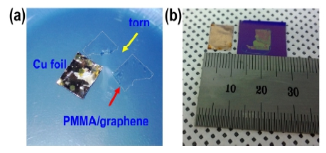
Fig. 1
H2 bubbling process using a 5 wt% PMMA solution in toluene as a supporting layer. Photographs of (a) the floated PMMA/ graphene stack on a 0.1M NaOH aqueous solution after detaching from a Cu foil and (b) the transferred PMMA/graphene stack onto a SiO2/Si. In the case of thin PMMA film used as a supporting layer, PMMA/graphene stack is broken to pieces due to intense H2 bubbles generated at the interface between Cu foil and PMMA/graphene.
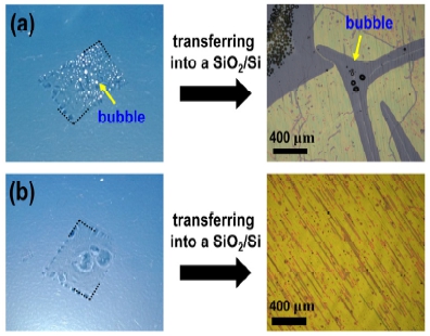
Fig. 2
Bubbles under PMMA/graphene stack are inevitably formed in this H2O electrolysis, as shown in the photograph in (a). If bubbles are not removed, wrinkles induced by bubbles were formed on PMMA/graphene stack after transferring into SiO2/Si, as shown in the OM image in (a). Therefore, the process of removing bubbles under the PMMA/graphene stack is essentially needed for conformal contact with the substrate, as shown in (b).
Following the H2 bubbling transfer process onto a SiO2/Si, the morphological characteristics of the transferred graphene films such as torn and folded graphene regions were investigated by an optical microscope (OM; Nicon, ECLIPSE LV150) with a halogen lamp using the contrast difference between the SiO2 and graphene area. The structural qualities of as-grown and transferred graphene films were confirmed by Raman spectroscopy. Raman spectra were obtained by a WiTec alpha 300R M-Raman system with 532 nm (2.33 eV) excitation. The laser spot size, when focused, was ~500 nm in diameter with a 50× optical lens. After the H2 bubbling transfer process, PMMA residues and remaining contaminations on the graphene were investigated using X-ray photoelectron spectroscopy (XPS). The XPS studies were conducted on a K-alpha spectrometer (Thermo Fisher) using Al Kα nonmonochromatic X-ray excitation at a power of 72 W, with an analysis area ~0.4 mm in diameter and a pass energy of 50 eV for electron analysis.
3. Result and Discussion
Fig. 3(a) shows a representative OM image of the graphene film transferred onto a SiO2/Si using the H2 bubbling process, in which the PMMA/graphene/SiO2 was heated at 50 °C on a hot plate, followed by removing the PMMA layer by acetone. In this OM image, regular striped patterns with bright purple colours are observed, in contrast to the conventional wet etching transfer method using iron chloride or an ammonium persulfate aqueous solution.6,7) These striped patterns are reduced as the temperature of baking the PMMA/graphene/ SiO2 after scooping the detached PMMA/graphene is increased to 150 °C, as shown in Fig. 3(b). To identify these striped patterns, we have performed Raman measurements on the striped regions and other areas in the transferred graphene layer. As shown in Fig. 3(c, d), a Raman spectrum taken from the dark purple areas [a blue spot in Fig. 3(c)] shows three primary features: a D band at ~1,351 cm-1, a G band at ~1,592 cm-1 and a 2D band at ~2,685 cm-1, all expected peak positions for graphene.9-11,13) In addition, we obtained the ratio of the G-to-2D peak intensities (IG/I2D), determining it to be ≤ 0.5, while also finding a full-width-at-half-maximum (FWHM) value of ~30 cm-1 for the 2D band with ID/IG ≤ 0.1, suggestive of a monolayer graphene sheet with a relatively low defect density. However, in the bright purple area [a black spot in Fig. 3(c)], there are no peaks in the Raman shift range from 1,100 to 3,000 cm-1. Based on those results, the graphene layer is not present on the regions of stripped patterns and thus causing the contrast difference between the graphene and SiO2 surface due to the constructive interference at visible light.
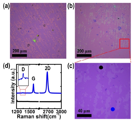
Fig. 3
Representative OM images of graphene films transferred onto SiO2/Si substrates after baking the PMMA/graphene/SiO2 (a) at 50 °C and (b) at 150 °C and then removing the PMMA layer by acetone, respectively. (c) A higher magnification OM image obtained from the red square in (b). (d) Raman spectra taken from black and red spots in (c).
Considering that, in our growth conditions, the graphene layer fully covers a Cu foil surface without any empty areas, the above results indicate that the continuous as-grown graphene layer on a Cu foil is partially torn or disappeared during the transfer process by using H2 bubbles. Here, key questions are at which stage the graphene sheet is severely torn during this H2 bubbling transfer process and what may be the origin of this tearing phenomenon. There are two possible routes for inducing the degradation of the transfer efficiency of as-synthesized graphene films onto the desired substrate when using the H2 bubbling transfer process: (i) after detaching the PMMA/graphene stack from the Cu surface, some graphene areas remain on the Cu surface still and/or the graphene attached to the PMMA supporting layer comes away during this transfer process due to a lot of bubbles generated from a water electrolysis process, and (ii) when removing the PMMA layer using acetone after scooping the detached PMMA/graphene stack into a substrate, some regions of the graphene are ripped due to the weak adhesion between the graphene and the target substrate.
For the first time, we checked the remaining Cu surface after the H2 bubbling transfer. From the OM image in Fig. 4(a), the morphologies of the remaining Cu surface do not change significantly after detaching the PMMA/graphene bundle, comparing to a bare Cu foil [an inset in Fig. 4(a)]. In the Raman study, we determined that there are no characteristic Raman signals related to the graphene, such as the G or the 2D band, on the overall Cu surface after the transfer process [as shown in Fig. 4(b)]. However, in the SEM image of the backside of the PMMA/graphene stack, several wrinkles [blue arrows in Fig. 4(c)], which are originated from the thermal expansion coefficient difference between the graphene and the Cu during the cooling stage in graphene growth procedure,6,9) as well as multi-layer graphene regions [the red dotted circle in Fig. 4(c)], are observed. In addition, the Raman spectra acquired from the backside of the PMMA/ graphene stack clearly show the unique characteristics of graphene: a G band at ~1,592 cm-1 and a 2D band at ~2,685 cm-1 [as shown in Fig. 4(d)]. These results indicate that the as-grown graphene layer on a Cu foil is not only fully moved into the PMMA supporting layer but also stably adheres to it without any degradation or tearing of the graphene layer during the H2 bubbling process. Therefore, in the whole H2 bubbling transfer process, the graphene films are most commonly torn while removing the PMMA supporting layer, imposing limitations on a variety of electronic and optoelectronic applications required for large-area, continuous graphene films.
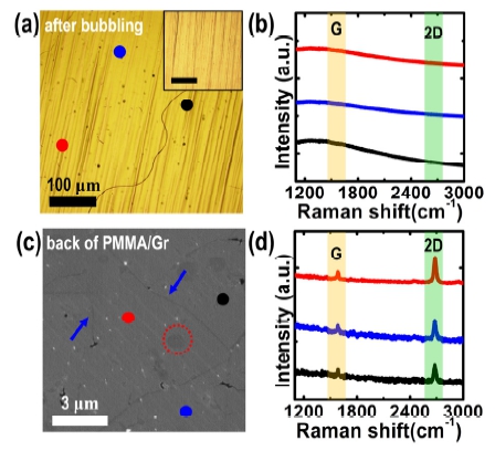
Fig. 4
(a) A typical OM image of the Cu surface after detaching the graphene layer from the graphene/Cu stack using the H2 bubbling transfer technique. Inset in (a) is an OM image of a bare Cu foil for comparison (scale bar; 50 μm). (b) Corresponding Raman spectra obtained from black, blue, and red spots in (a). (c) A representative SEM image of the back side of the PMMA/graphene bundle separated from a PMMA/graphene/Cu foil by the H2 bubbling process. (d) Corresponding Raman spectra obtained from black, blue, and red spots in (c).
Two other important questions remain to be answered: (i) what caused the graphene films to be torn while removing the PMMA layer, and (ii) what is a simple remedy for this problem? In order to answer these questions, first, we investigated the surface morphology of the graphene/Cu and the detached PMMA/graphene on a SiO2/Si by means of OM and atomic force microscopy (AFM). As shown in Fig. 5(a), although the Cu was annealed at 1,000 °C, close to the melting point of the Cu bulk for the graphene growth, numerous inherent rolling textures of a Cu foil produced by the coldrolled method still remain, showing a saw-tooth shape in cross-sectional line profile images [a right panel in Fig. 5(a)]. From the AFM line profile, we confirm that the width between apexes and the height from the groove to the apex are 18.6 ± 5 μm and 337 ± 66 nm, respectively. After spincoating a PMMA solution onto this graphene/Cu, followed by detaching it using the H2 bubbling process, the PMMA/ graphene stack transferred onto the SiO2/Si also shows similar morphological features, although the height of the rolling features is reduced to ~170 nm [as shown in Fig. 5(b)]. Given these morphological characteristics of the PMMA/graphene stack transferred onto SiO2/Si, we could expect that the PMMA/graphene around the vertex of the saw-like shape loosely adheres to SiO2/Si or is suspended. As a result, during the process of removing the PMMA layer using acetone, graphene regions around the vertex in the PMMA/graphene are selectively torn and thus form regular stripe patterns, which is similar to the phenomenon observed in the process of creating suspended graphene on a membrane with micrometer- sized holes.14) It is highly noted that the thick PMMA film as a supporting layer should be required in the H2 bubbling transfer process, as mentioned above in Fig. 1, and this severely hinders the conformal contact to the flat substrates.
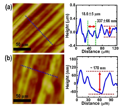
Fig. 5
AFM images and corresponding line profiles of (a) a graphene/ Cu surface and (b) a PMMA/graphene stack transferred onto a SiO2/Si using the H2 bubbling transfer process. The line profiles were obtained from blue dotted lines in (a) and (b), respectively.
To solve this problem caused by the morphological characteristics of the corrugated PMMA/graphene layer, we applied pressure to the PMMA/graphene/SiO2 assembly together with heating at temperatures ranging from 50 and 150 °C using a home-built heat press equipment in an effort to improve the adhesion to the target substrate, as shown in the schematic illustration in Fig. 6(a). It is important to note that, in this method, the optimal pressure (in our case, P ~0. 03 MPa) is a key parameter for the transfer of graphene without cracks induced by the expansion of the PMMA/graphene assembly for pressing. Fig. 6(b) shows a typical OM result of the transferred graphene on a SiO2/Si obtained at a pressure of ~0.03 MPa and a temperature of 100 °C. There are no graphene tearing features that are normally observed in the H2 bubbling transfer process without a hot-pressing procedure. This result indicates that the hot-pressing procedure improves the adhesion properties between the PMMA/graphene assembly and the SiO2/Si, especially, at the apex regions of the PMMA/graphene layer.
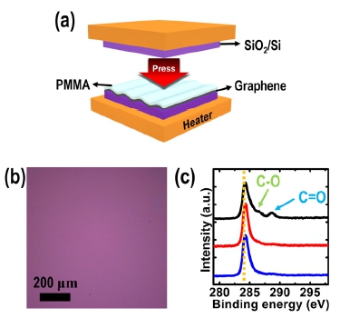
Fig. 6
(a) A schematic diagram of the heat-press-transfer method. (b) A representative OM image of the transferred graphene layer onto a SiO2/Si assisted by the hot-pressing at 100 °C. (c) XPS C1s high-resolution line scans of the transferred graphene films pressed at temperatures of 50 °C (blue line), 100 °C (red line), and 150 °C (black line) from bottom to top.
Moreover, with regard to this process, we investigated the effect of the temperature under a constant pressure of ~0.03 MPa on graphene transferability using OM and X-ray photoelectron spectroscopy (XPS). In Fig. 6(c), the high-resolution C 1s line-scan spectra obtained from graphene surfaces after the removal of the PMMA layer pressed at 50 °C (blue line) and 100 °C (red line) exhibit a dominant peak at ~284.5 eV, corresponding to graphite-like sp2-hybridized carbon and therefore indicating that most of the carbon atoms retain a two-dimensional honeycomb backbone structure.15) However, when the PMMA/graphene stack is pressed at ~150 °C, we can detect two additional carbon peaks located at ~285.5 and ~288.2 eV, which could be attributed to oxygen functionalities such as epoxide and carbonyl groups, respectively [black line in Fig. 6(c)].16) These oxygen functional groups may originate from the PMMA residue, which forms covalent bonds with graphene at defect sites above the glass transition temperature of PMMA, causing the degradation or modification of the intrinsic properties of graphene.15) Therefore, temperature is also an important factor in the heat-pressassisted transfer method.
4. Conclusion
In conclusion, we systematically studied the tearing phenomenon during the H2 bubble-assisted transfer process of a graphene layer grown on Cu foil using several types of surface analysis equipment. In this study, our experimental results strongly suggest that inherent rolling features of Cu foil cause the saw-like corrugation of the PMMA/graphene stack when transferred onto the substrate after the Cu is dissolved. Thus, graphene tearing mainly appears at the apexes of corrugation due to weak adhesion to the substrate. We devised a simple and effective method that relies on a heat press technique to resolve this tearing problem. We found that, with this method, the optimal pressure and temperature conditions were the key parameters to obtain large-area and high-quality graphene without defects or contamination induced by the graphene transfer process.
