

1. Introduction
At the beginning of the twentieth century, physicists developed a new technique for cooling materials to a temperature close to absolute zero (-273 °C) and began the process of discovering the properties of materials and their ability to conduct electricity in such critical conditions. In some elements, such as mercury and lead, scientists noticed something surprising, which is that at a certain temperature, these materials become electrically conductive without any resistance. Tens of years after this discovery, similar properties were found for thousands of compounds, from ceramics to carbon nanotubes. This state of matter is called a superconductor. Superconducting materials conduct the electric current without any resistance and experiments were conducted to verify this and it was found that a wire of superconducting material in the form of a loop in which the electric current continued for a very large period, and the current is expected to continue for billions of years without any loss. On the microscopic scale, the electrons of superconducting materials behave completely differently than they do in conducting metallic materials. Electrons in superconducting conductors are paired with each other, allowing them to move easily through the material. This is a bit like a commuter route on a highway. Single electrons suffer from high resistance due to their continuous collisions with the nuclei of atoms, which makes their movement inside the material surrounded by many collisions, but in the case of paired electrons, they have a special path inside the material without suffering from collisions with the nuclei of the atoms.1)
There are many different applications for superconducting materials, for example, magnetic resonance imaging (MRI) machines. MRI machines use superconducting materials to generate a large magnetic field that allows them to obtain images inside the patient's body. For more information, see the article How MRI works. The magnetism of superconducting materials also made it possible to detect Higgs Boson particles at CERN by controlling the paths of colliding particles.2) It is well demonstrated that materials exhibiting high temperature superconductivity (HTS) reveal the possibility to produce a magnetic field exceeding that of achievable via low temperature superconducting ones.3) Cuprate-based superconductors are of essential importance in wide range of technological and industrial applications. In 1986, Bednorz and Müller4) have synthesized BaLaCuO superconductor in the form of BaxLa5−xCu5O5(3−y) with x = 1 and 0.75, y > 0. This polycrystalline phase revealed perovskite type structure with critical temperature (Tc) at about 30 K. This discovery has paved the way to search for another high temperature superconducting materials such as YBa2Cu3Ox with superconductivity at 93 K.5) Furthermore, Bismuth-based cuprate BiSrCuO is another family of superconductors.6) In addition, the crystallography of Bi2Sr2CaCu2O8 shows the existence of two CuO2 layers disjointed by a Ca layer and of rock - salt like Bi2O2 layers. While the (CuO2)Ca· (CuO2) layers are disconnected by single SrO layers from the Bi2O2 layers.7) Superconductivity behavior at higher than 150 K in HgBa2Ca2Cu3O8+δ was recorded.8) Fabricating new cuprate superconductors with Tc higher than liquid nitrogen temperature (77 K) has been the main motivation of researchers mainly via introducing a variety of elements. Early studies showed that the replacement of Bi by Ag, Nb and Sb in the Bi-Pb-Sr-Ca-Cu-O system improved the superconducting Tc near 115 K.9) The zero resistivity performance and the superconducting critical temperature above 120 K of the Ca‐Ba‐Cu‐O system is achieved by introducing Tl.10) Our research group have studied the impact of substituting Ba with Sr and Tl with Pb of Tl0.6Pb0.4Ba2−xSrxCa2Cu3O9−δ superconductor system at x = 0, 0.1, 0.2, 0.3, 0.4 and 0.5. The optimal recorded Tc (offset) was about 113 K for the composition Tl0.6Pb0.4 Ba1.5Sr0.5Ca2Cu3O8.76.11) The conventional sold state reaction is utilized to prepare Tl0.5Pb0.5Ba2Can-1Cun-x NixO2n+3-δ at n being fixed to 3 with the variant contents of x at 0, 0.2, 0.4, 0.6, 0.8 and 1. The maximum observed critical temperature Tc corresponded to 139 K at x = 1.10) Two groups of superconducting samples of Bi1.6Pb0.4Sr1.8Ba0.2Ca2Cu3O10+d were fabricated and quenched in air and liquid nitrogen. Findings reveal that higher Tc was detected for air quenched samples.13)
To this end, the current study is the first to report the synthesis of Pb2Ba1.7Sr0.3Ca2Cu3O10+δ ceramic superconductor followed by the evaluation of lattice strain and crystallite size utilizing several methods namely, Scherrer, Williamson-Hall (W.H), size-strain plot (SSP) and Halder Wagner (H.W).
2. Experimental Procedure
Pb2Ba1.7Sr0.3Ca2Cu3O10+δ phase has fabricated using solid-state reaction, the samples were prepared according to the following steps;
1. Using appropriate weights of pure (99.998 %) materials of Pb2O3, BaO, SrO, CaO and CuO, (May & Baker LTD Dagenham England) with their proportional molecular weights.
2. A sensitive scale (Mettler H35 AR with maximum loading of 110 g and readability of 0.001) has been utilized to measure the weight of each reactant.
3. The powders BaO, SrO, CaO and CuO have been assorted together utilizing a gate mortar slurry. An adequate amount of 2-propane has added to homogenize the combination and produce a slurry during the grinding procedure for approximately (40-60) minutes.
4. The mixture was calcinations in a Furnace at 700 °C for five h and this heat treatment was done to remove the oxides and unwanted substances from the mixture. For this process, the mixture being with black color was taken out.
5. The powder was re-grinded again, to remove all gases from the mixture.
6. Then, the powder has been pressed into disc-shaped pellets of 1.5 and 0.5 cm in diameter, via a hydraulic press (Specac) under pressure of 6 tons / cm2.
7. The synthesized samples were positioned in an electric furnace at 860 °C for 24 h with heating rate of 60 °C per hour heating rate and the samples, subsequently, were cooled down at the same heating rate until room temperature. The structure of the fabricated sample has been acquired operating Philips-type X-ray diffractometer (XRD) which uses Cukα source with λ = 1.5405 Å, generating current of 20 mA and voltage 40 KV. The phase transformation of several structures was studied using XRD to obtain the properties of the structure. The crystallite size (D) and the lattice strain (e) were computed by angles and widths of the intensity of the XRD peaks. XRD results were refined by Fullprof, Mach!, Origin and VESTA software,14) to compute the lattice dimensions represented by a, b and c, crystallography type , distance space (dhkl), full width at half maximum (FWHM) and degree of crystallinity. Nano particles was evaluated by W.H, SSP and H.W models and the findings of crystallite size attained via the aforementioned methods were compared with the method of Scherrer. Furthermore, a four-probe procedure has been implemented to determine the electrical resistance (ρ) as a function of temperature to determine the critical temperatures Tc(onset), Tc(off set) and transition width ΔT at temperature of (77-300 K). The work procedure is described elsewhere.15)
3. Theoretical Part
The corrected expansion has been assessed using βhkl by applying the Gaussian function.16,17)
Scherrer's equation displays the amplitude of the XRD pattern being ascribed to the widening caused by the crystallite size. βhkl represents FWHM of the sharpest Pb2Ba1.7Sr0.3Ca2Cu3O10+δ peak lines revealed in Fig. 1. K is Scherrer's constant, which equals 0.94, D denotes the crystallite size. λ and θ signify X-ray wavelength, and the Bragg angle, correspondingly.17,18)
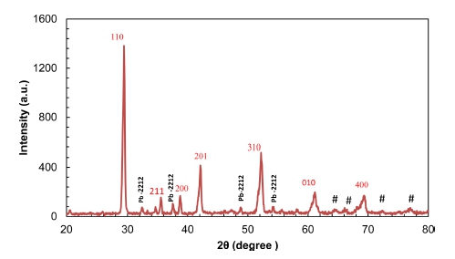
Fig. 1
XRD pattern of Pb2Ba1.7Sr0.3Ca2Cu3O10+δ (Pb-2223 phase) compound with minor amount of Pb-2212 phase and impurities (#) at higher diffraction angles.
The collected data via W.H method regarding the lattice strain (ε) and the crystallite size (D) of Pb2Ba1.7 Sr0.3Ca2Cu3O10+δ was achieved from βhkl deploying the W.H relationship. Micro strain enlargement in the W.H method is shown below;17)
The total broadening of a line peak βhkl in W.H approach is sum of the size and micro strain widening, so the entire βhkl can be expressed;19)
Here K refers to Scherrer's constant or shape modulus equal to 0.94 for spherical particles and ε corresponds to the internal micro strain.
On the other hand, when using SSP model, ε and D of Pb2Ba1.7Sr0.3Ca2Cu3O10+δ compound can be calculated from βhkl and the planar spacing dhkl (the space between contiguous atomic levels) using SSP method. The SSP model is more precise, particularly at higher yaw angles. Consequently, the crystallite size (D) and lattice strain (ε) of the studied compound were assessed utilizing SSP model. In this manner, the amplitude of the peak that is belonging to the network strain is calculated by ε = βs ∕ tanθ.20) Accordingly, the overall broadening is reported as;
Based on SSP model, the relationship between lattice strain (ε) and crystallite size (D) is reported.
Here; K represents the shape modulus amounts to 3/4 for spherical particles.
The information concerning the microstrain (εH.W), and crystallite size (DH.W) of Pb2Ba1.7Sr0.3Ca2Cu3O10+δ compound is determined from βhkl and the planar spacing dhkl (distance between neighboring levels in the group (h k l) using the H.W method. This approach gave an approximation of the integral view of the Voigt function as follows:
In the above equation, βL and βG symbolize the components of Lorentzian and Gaussian, correspondingly. The crystallite size (D) and strains profiles were demonstrated using Lorentzian and Gaussian function, in that order. Accordingly, the equation below is displayed;21)
4. Results and Discussion
XRD pattern of the Pb2Ba1.7Sr0.3Ca2Cu3O10+δ superconductor is presented in Fig. 1. A slight splitting of the peaks detected at ~ 29.4°, ~ 35.55°, ~ 38.75°, ~ 42.1°, ~ 52.25°, ~ 62.15° and ~69.2° is indicative of a specific existing system. XRD data was analyzed using the Mach!, Origin and VESTA software’s. Determining the type of structure confirms the perovskite structure out the presence of addition phases. When comparing the X-ray diffraction of the standard charts with the XRD pattern of the obtained sample, we noticed that the Pb2Ba1.7Sr0.3 Ca2Cu3O10+δ sample matches well with the Pb-2223 phase with minor amount of Pb-2212 phase and impurities (#) at higher diffraction angles. After calculating the lattice constants (a, b and c) using Fullprof software it was found out that all the XRD pattern peaks correspond to the pseudo-tetragonal structure. The attained result also demonstrates that the best fitting for the obtained results was implemented as shown in Fig. 1. In order to carry out rietveld optimization via Fullprof software, accurate values of lattice constants and the space group type acquired from XRD test which were subsequently refined by Mach and Origin software, are required. The lattice constants are reported to be a = 3.732, b = 3.733 and c = 14.75 Å. Subsequently, a comparative investigation of the average crystallite size for Pb2Ba1.7Sr0.3Ca2Cu3O10+δ estimated by XRD powder is reported. The microscopic strain caused by the lattice deformation of Pb2Ba1.7Sr0.3 Ca2Cu3O10+δ nanoparticles was computed by W.H, SSP and H.W approaches and the findings for crystallite sizes (D) extracted by these three methods were compared with Scherrer method.16) In all of these methods, the βhkl values of XRD peaks are determined from the findings collected from Rietveld refinement utilizing Fullprof software which is belonging to the 5 strongest Pb2Ba2Sr2 Cu3O10+δ peaks as displayed in Fig. 1. In addition, the distance between neighboring levels, dhkl values are computed by Bragg equation, nλ = 2d sinθ in which λ = 1.540440 Å.
4.1. Scherrer's method
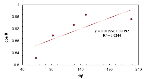
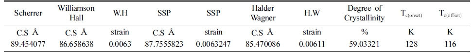
In Scherrer's method (equation 1), the values of βhkl and the cosθ of the angle corresponding to 5 peaks were calculated. Then, the results were plotted (Fig. 2) and by calculating the slope of the straightforward line the crystallite size values were found as shown in Table 1. In Scherrer's method, the rise in the amplitude of the peak is because of the drop in the size of the crystals. Scherrer's equation is utilized to determine the size of crystals from Gaussian line profiles.17,18) However, the equation is not anticipated to be accurate for crystallite sizes that are smaller than 10 nm (<10 nm). D values for the 5 analyzed peaks obtained by Scherrer’s method is tabulated in Table 1. From the table, Crystallite sizes of the peaks at smaller angles (2θ) are more accurate.
4.2. Williamson-Hall (W.H) method
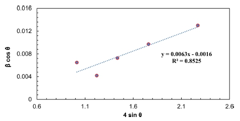
In this method and according to equation 4, cosθ βhkl values of the five strongest peaks of Pb2Ba1.7Sr0.3Ca2 Cu3O10+δ have been plotted against 4sinθ values and shown in Fig. 3. The slope and the intersection of the linearly fitted data reveal of small amounts of lattice strain (ε) and crystallite size (D), correspondingly. Negative microscopic stress tends to be due to lattice contraction. Substantially, the larger the crossover result, the smaller the crystallite size, and the larger the slope the greater the microscopic stress. The objection with the origin means that crystallite size is infinity or that the widening is because of the expansion of the micro strain and the zero regression means that the horizontal line without micro strain or the broadening is ascribed to the enlargement of the crystallite size, D.21) The crystallite size (D) and microscopic stress for the five main peaks acquired from the Williamson-Hall model are calculated and listed in Table 1.
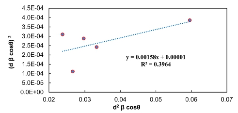
4.3. The Size-Strain Plot (SSP) method
From equation 6, (dhkl βhkl cosθ)2 values have been plotted versus (d2hkl βhkl cosθ) values for the five main peaks of Pb2Ba1.7Sr0.3Ca2Cu3O10+δ as demonstrated in Fig 4. The results in the figure were linearly fitted and then the crystallite size (D) is estimated from the slope of the fitted line of the plotted data. Furthermore, the root of the y-intercept discloses the micro strain (ε). The related results of D and ε of the main peaks obtained from SSP method and depicted in Fig.4 are summarized in Table 1.
4.4. Halder Wagner (H.W) method
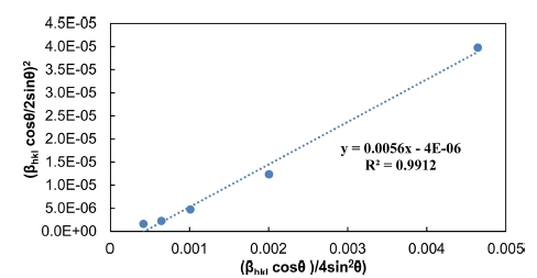
In H.W method, the plot of (βhkl cosθ/2sinθ)2 values of the main peaks were plotted against (βhkl cosθ)/4sin2θ) values as displayed in Fig. 5 is a direct line with positive slope and a non-zero y-intercept. The crystallite size (D) was predicted from the inverse value of the slope of the linearly fitted data and the square root of y-intercept determines the exact strain, respectively. The crystallite size and microscopic stress main peaks extrapolated from H.W model are reported in Table 1. The results for the crystallite size and micro strain analysis of Pb2Ba1.7Sr0.3 Ca2Cu3O10+δ compound assessed by Scherrer, W.H, SSP and H.W models are listed in Table 1. All methods demonstrate that the line expansion was fundamentally distinguished. W.H method assumes that the crystallite size (D) and the micro strain profiles participate to line enlargement with Lorentzian profiles but in both SSP and H.W methods. Moreover, it is presumed that the crystallite size (D) and micro strain profiles are designated by the Lorentzian function and the Gaussian function, respectively.17) In comparison with Scherrer and W.H, both SSP and H.W models have the benefit that fewer weights is set to the data from reflections at high angles. However, given the R2 values written within Figs. 2-5, it is indicated that the H.W model involves highest accuracy, when the entire data points aligning the fitting line. Further, this method has minimal micro stress.18) Therefore, it can be concluded the most accurate method is associated with R2 value being close to 1 or in other words, the method yields x-y data points which touch or closest to the fitting line.
4.5. Crystallinity
The degree of crystallization of many materials can be assessed using crystallography analysis with the help of X-ray diffraction. Crystallization is generally calculated as a percentage of the volume of the crystalline substance. However, the degree of structural perfection can vary even within fully crystalline materials. The degree of crystallization could be measured using X-ray crystallography based on the following equation:
Entering the data taken from the VESTA software was calculated. It was found that the degree of crystallization is 59.03321 % as displayed in Table 1.
4.6. Resistivity
The electrical Resistivity was examined as a function of temperature change using the four-probe method. Fig. 6 plots the electrical resistivity values versus temperature for Pb2Ba1.7Sr0.3Ca2Cu3O10+δ compound. From the Figure, it is obviously observed that the electrical resistivity curve reduces as the temperature decreases. This indicates the behavior of the metal.22,23) It is also noted that the curve shows a transition from the normal state to the superconducting state, so that the critical temperature is determined at the first drop of the curve Tc(onset) (the temperature at which the transition from the normal state to the superconductor state begins) is at 128 K and the critical temperature at the zero resistivity Tc(off set) is detected at 116 K, the change in transition width (ΔT = 12 K) as reported in Table 1.
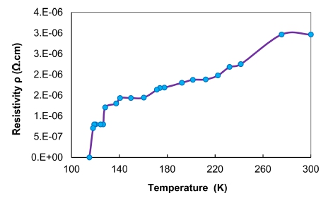
We conclude from the foregoing that the results obtained in this paper correspond in terms of content with the results in references24,25) with the difference in values, because the Pb2Ba1.7Sr0.3Ca2Cu3O10+δ compound under experiment differs in behavior and structure if compared with other compounds references.
5. Conclusions
In this work, structural and characterization of Pb2Ba1.7 Sr0.3Ca2Cu3O10+δ compound synthesized by solid-state method were examined by X-ray powder diffraction scan. The data of Mach!, Origin and VESTA software program to analyze the XRD spectra confirm the tetragonal structure. Moreover, the determined crystallite size (D) and micro strain (ε) of Pb2Ba1.7Sr0.3Ca2Cu3O10+δ material calculated by the Scherrer, W.H, SSP and H.W methods display that the H.W method is more precise due to the value of R2 is close to 1 with all data points which are touching the fitting line. It was found that the degree of crystallization is 59.03321 %. Finally, the resistivity curve demonstrates that the critical temperature Tc(onset) is at 128 K and the critical temperature at the zero resistivity Tc(off set) is 116 K, the alteration in transition width corresponds to ΔT = 12 K. This indicates that the synthesized compound possesses superconducting properties with a transition temperature above the liquid helium temperature, which confirms that the superconducting compound exhibits high transition temperature.
