


1 Introduction
GaN is a promising material for the applications to electronic devices such as high-power, high-temperature and high-frequency devices because of its large band gap, high electron saturation velocity, and high breakdown field.1,2) Successful realization of these devices strongly requires Schottky contacts with low reverse current and ohmic contact with low contact resistance. There have been various researches on the metal-insulator-semiconductor( MIS) Schottky diodes in order to obtain lower leakage current and higher rectification ratio.3-8) High performance metal-oxide-semiconductor field effect transistors (MOSFETs) can also be realized by combining GaN with high-k dielectric materials such as Al2O3.9) However, high interface trap density in Al2O3/GaN interface is known to be a big problem in device performance,10) which requires to minimize the interface trap density.
As a new passivation method in AlGaN/GaN device, atomic layer deposition(ALD) grown AlN layer has been studied due to its good isolation stability and high interface quality in AlGaN/GaN.11-13) Huang et al. suggested in GaN on Si with Al2O3/AlN dielectric stack that highdensity positive fixed charges induced by AlN thin film can compensate the acceptor-like interface traps, resulting in effective suppression of current collapse.11) The AlN passivation effect was found to be more significant in the interface properties in Al2O3/GaN for m-plane GaN as compared to c-plane GaN.12) In our previous work, we applied ultrathin AlN layer to Al2O3/GaN using ALD and investigated the interfacial and electrical properties of Al2O3/AlN/GaN MIS diodes with different Al2O3 thicknesses and found that Al2O3 thickness is a key factor in device performance.13) However, we did not analyze the X-ray photoelectron spectroscopy(XPS) characteristics at different etch depths and current-voltage(I-V) characteristics were obtained at room temperature only. In this respect, we investigated the interfacial properties using XPS at different etch depths and the temperature dependent current transport to get the detailed interfacial formation mechanism in Au/Al2O3/AlN/GaN MIS diodes.
2 Experimental
Hydride vapor phase epitaxy(HVPE)-grown, c-plane (0001) bulk GaN wafer(thickness: 300 μm, carrier concentration: 5 × 1014cm−3) purchased from Lumilog. was used in this work. The wafer was cut into small pieces and some of them were loaded into an ALD chamber after cleaning process. Then, the temperature was ramped up to 350 °C to deposit 1 nm thick AlN layer using Trimethylaluminum(TMA) and NH3 as precursors. After that, the temperature was reduced to 250 °C to grow 5 nm thick Al2O3 layer using TMA and H2O as precursors. The thicknesses of AlN and Al2O3 films on the Si witness samples were measured using a FS-1 multi-wavelength ellipsometers, acquiring ellipsometric ψ(amplitude ratio) and Δ(phase angle) data at 4 wavelengths across the visible spectrum: 465, 525, 580, and 635 nm. Measured data were fitted using a least-squares algorithm. In other words, the agreement between the experimentally measured and the calculated ellipsometric data was quantified by the Fit Difference, summed over all 4 measurement wavelengths. To observe the formation mechanism near the Al2O3/AlN/GaN interface, XPS measurements with sputter etch treatment were performed using a monochromatic Al Kα x-ray source(1486.6 eV). The collected data at three different etch depths(interval: 1 nm) were analyzed with the multiple Gaussian functions. For Schottky contacts, 50 nm thick Au metal films were deposited by using electron beam evaporation through a shadow mask. For substrate back contacts, 100 nm thick Al metal was deposited using electron beam evaporation and In metal was rubbed over the entire back surface to attach the samples on the Cu plate. Temperature dependent currentvoltage( I-V-T) measurements were carried out with a Keithley 238 current source after placing samples on a hot chuck connected with a temperature controller.
3 Results and Discussion
Fig. 1 shows the Ga 3d core level spectra near the Al2O3/AlN/GaN interface. The peaks were decomposed into four components. The main peak at ~19.8 eV is associated with Ga-N.14) The peaks at ~18.5 eV, ~19.0 eV and ~20.5 eV can be attributed to metallic Ga(Ga-Ga), Ga2O and Ga2O3, respectively.15) The additional peak at higher energy(~21.0 eV) was assigned to the oxide in Ga-O bonds.16) This peak also will be related with Ga in Ga2O3.17) The integrated intensity ratios of Ga-O/Ga-N were calculated to be 0.29, 0.28, and 0.88, respectively, for the depths 1, 2, and 3 (i.e., deeper from the surface). This indicates that Ga2O and Ga2O3 are present significantly near the AlN/GaN interface, resulted from the Ga native oxide on GaN surface. During the ALD deposition process, these Ga-O bonds might be removed due to the self-cleaning effect through ALD process. Brennan et al. investigated the initial stage of Al2O3 growth on AlGaN surface by XPS and suggested that Al2O3, Ga2O3, and NO states present initially were reduced during the course of the deposition process.18) In addition, similar values for depths 1 and 2 imply that such reduction of Ga-O bonds occurred during the earlier ALD growth stage. This clearly indicates the removal of native oxide on GaN surface by AlN layer.

Fig. 2 shows the Al 2p core level spectra, which are deconvoluted into four components. The main peak at ~75.0 eV are associated with Al2O3.10) The peak at higher binding energy(~76.0 eV) corresponds to the Al(OH)3 state10,19) and the peak at ~73.5 eV is related with AlN.20) By increasing rapid thermal annealing(RTA) temperature, the Al(OH)x concentration was found to decrease in Al2O3/ AlGaN/GaN high electron mobility transistor(HEMT), which suppressed the threshold voltage(Vth) shift.21) Hence, the removal of Al-OH bonds is beneficial in device performance. The presence of Al-OH is possible during the Al2O3 growth using TMA and H2O as precursors because some of hydroxyl groups are incompletely removed during the reaction cycle. The integrated intensity ratios of Al-OH/Al2O3 were calculated to be 0.50, 0.72, and 1.92, respectively, for the depths 1, 2, and 3. This implies that the removal of hydroxyl groups were accelerated as the Al2O3 growth proceeded. Additionally, the peak at ~74.5 eV may be due to the formation of unstable defective oxide such as Al2O and AlO acting as interface states.10) The peak may also be associated with the Al-O-N bonds,22) which can occur due to the presence of diffused N atoms.

Fig. 3 shows the O 1s core level spectra, which are deconvoluted into three or four components. The peak at 531.7-532.0 eV is associated with Al2O3.23) The peaks at ~530.7 eV and ~531.0 eV are associated with Ga-O bonding in Ga2O3,24,25) which might be due to the diffusion of Ga atoms into Al2O3 layer. The peaks observed at higher energy(532.7-533.6 eV) can be associated with Al-OH.26) The integrated intensity ratios of Al-OH/Al2O3 were calculated to be 0.26, 1.95, and 2.56, respectively, for the depths 1, 2, and 3, showing the same trend as obtained from the Al 2p core level spectra. This again indicates that the generation of Al-OH related defects were suppressed during the Al2O3 growth process.

Fig. 4(a) shows the forward I-V curves measured at different temperatures. Based on the thermionic emission (TE) model,27) the temperature dependences of the barrier height and the ideality factor has been obtained, which is shown in Fig. 4(b). The ideality factor is much larger than unity, indicating that the tunneling current across the Al2O3/AlN bilayer is significant. The barrier height increased and the ideality factor decreased with increasing the temperature. Such temperature dependence is associated with lateral Schottky barrier inhomogeneity.26) According to inhomogeneous barrier model,27) the temperature dependent effective barrier height(φB) is related with a zerobias mean barrier height(φB) and a standard deviation(σ0) as φB = φB − qσ0 2/2kT. The linear fits to the plots of φB vs. 1/2kT shown in Fig. 5(a) yielded the values of φB = 1.182 eV and σ0 = 0.182 V. Fig. 5(b) shows the modified Richardson plots of ln(I0/T2) − q2σ02/2k2T2 vs. 1/kT. The intercepts at the ordinate produced the Richardson constant of A** as 30.45 Acm−2K−2, which is similar to the theoretical value of 26.4 Acm−2K−2 for n-GaN, indicating that the barrier inhomogeneity is appropriate to explain the current transport.
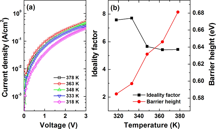
Fig. 4
(a) Semilogarithmic forward I-V characteristics at different temperatures and (b) obtained barrier height and ideality factor as a function of temperature.

Fig. 5
(a) Plot of barrier height vs. 1/kT and (b) modified Richardson plot of ln(I0/T2) − q2σ02/2k2T2 vs. 1/kT.
Growth of AlN interfacial layer between Al2O3/GaN layers are reported to block effectively oxygen from the GaN surface and prevent the formation of detrimental Ga-O bonds, enhancing the device performance.28) In-situ N2 plasma cleaning, consisting of alternating cycles of N2 plasma and TMA prior to Al2O3 deposition was found to passivate Al2O3/GaN interface states effectively, which was correlated with the suppression of Ga-O bonds and the formation of an aluminum oxynitride interfacial layer.29) N2 plasma pretreatment was also found to remove the native oxide on the III-N surface by forming an ultrathin monocrystal-like nitridation interlayer between Al2O3 and III-N surface.30) Gao et al. investigated the effect of TMA, H2O and Ar/N2 plasma pretreatment on the interfacial properties of Al2O3/GaN and found that TMA and H2O pretreatment had trivial effects on interface engineering whereas Ar/N2 plasma pretreatment slightly reduced interfacial trap density and significantly reduced the border trap density.31) Gu et al. reported that a two-step pretreatment, combining wet sulfide passivation with insitu cyclic TMA/H2 plasma exposure, was beneficial in reducing both interface and border traps for Al2O3/ GaN.32) From the XPS analyses, we also observed the removal of native oxide and the suppression of Al-OH bonds by AlN deposition. However, still the amount Ga- O and Al-OH bonds in Al2O3 cannot be negligible as seen from XPS data. These defects might increase the tunneling current significantly. Therefore, we expect that TMA/N2 plasma pretreatment prior to AlN deposition will improve the Al2O3/GaN interfacial quality further.
4 Conclusion
We investigated the interfacial properties of Al2O3/ AlN/GaN MIS diodes prepared by ALD. Based on the XPS analyses, it was found that the reduction of native oxides on GaN surface and the suppression of Al-OH bonds occurred, especially during the ALD early stage which corresponds to AlN deposition. The results indicate that AlN layer effectively blocked the formation of Ga-O and Al-OH bonds in Al2O3 layer. Temperature dependent I-V analyses revealed the barrier height increase with the temperature, which were associated with the lateral barrier inhomogeneity.