

1. Introduction
Magnesium and its alloys belong to the lightest group of engineering metals. Magnesium also has very attractive properties in strength to weight ratio, dimensional tolerance, 1-12) good electromagnetic shielding, damping capacity and machinability. Therefore, magnesium and its alloys are finding many applications in various industrial fields such as automobile, aerospace and communication technology. 13) However, the corrosion resistance of Mg alloy surface is very low in its natural state.1-6) Therefore, if the surface is not properly treated, the use of the Mg alloy is crucially limited by its inherent chemical activity. Accordingly, various surface treatment methods have been applied to solve this problems.
Among them, plasma anodizing is one of the most effective protection methods of the surface.1-11) In our, previous research on plasma anodizing of Mg alloys process parameters have been optimized mainly from the viewpoint of corrosion resistance. Desirable oxide films formed under the condition of pulse voltage mode as compared with DC mode.1,2)
Following the optimization of power mode, effect of electrolyte temperature on the corrosion resistance of the oxide film was studied.3) The corrosion resistance increased remarkably as the electrolyte temperature increased from 10 to 50 °C as indicated by rating number (RN) of 3.5 at 10 °C and 9.0 at 50 °C. The increase in corrosion resistance was ascribed to the decrease in defects in the oxide layer.
Thus, the electrolyte temperature plays an important role on the chemical nature of oxide films formed by plasma anodization. However, physical properties have not been examined in terms of electrolyte temperature for plasma anodization. In this study, the effect of electrolyte temperature for the formation of oxide film was investigated on the heat conduction property, dielectric breakdown voltage and wear behavior of the oxide film to optimize the condition for magnesium alloys to be applied as heat sink.
2. Experimental Method
As described in our previous work,1-3) AZ91D Mg alloy specimens with the chemical composition shown in Table 1 were used as anode (12 mm × 3 mm, thickness 3 mm) and a graphite plate was used as cathode. The plasma anodizing system consisted of electrolyte components, high voltage supply, high current pulse-reverse rectifier (NF, BP4650), cooler (Lab Companion, RW-1025G), and stainless steel (type 316) heat exchanger. Pulsed anodic voltage of 150 V was applied for 500 ms followed by 500 ms of rest time. The cycle was repeated for 30 min.

The surface, thickness, cross section and composition of the plasma anodized samples were examined using a field emission scanning electron microscope (FESEM). The specimen was cut, mounted in a cold place, and polished with silicon carbide (SiC) paper.
To measure dielectric breakdown voltage and thermal diffusivity, a withstanding voltage tester (model TOS5051A, KIKUSUI) and a laser flash analyzer (model LFA 457, Netzsch) were used, respectively.
In order to evaluate hardness, the samples were tested with a nanoindenter (model ENT-1100b, Elionix)
Wear test was carried out using an abrasion tester (Shinko zoki-sei, SSWT). Table 2 shows the test conditions.
Surface profile was measured using a surface roughness tester (MITUTOYO, SJ-400).
3. Results and Discussion
Figure 1 shows top views and cross-sectional images of the samples, treated at various temperatures and the energy-dispersive X-ray spectroscopy (EDS) element mapping of Mg, O and Si.
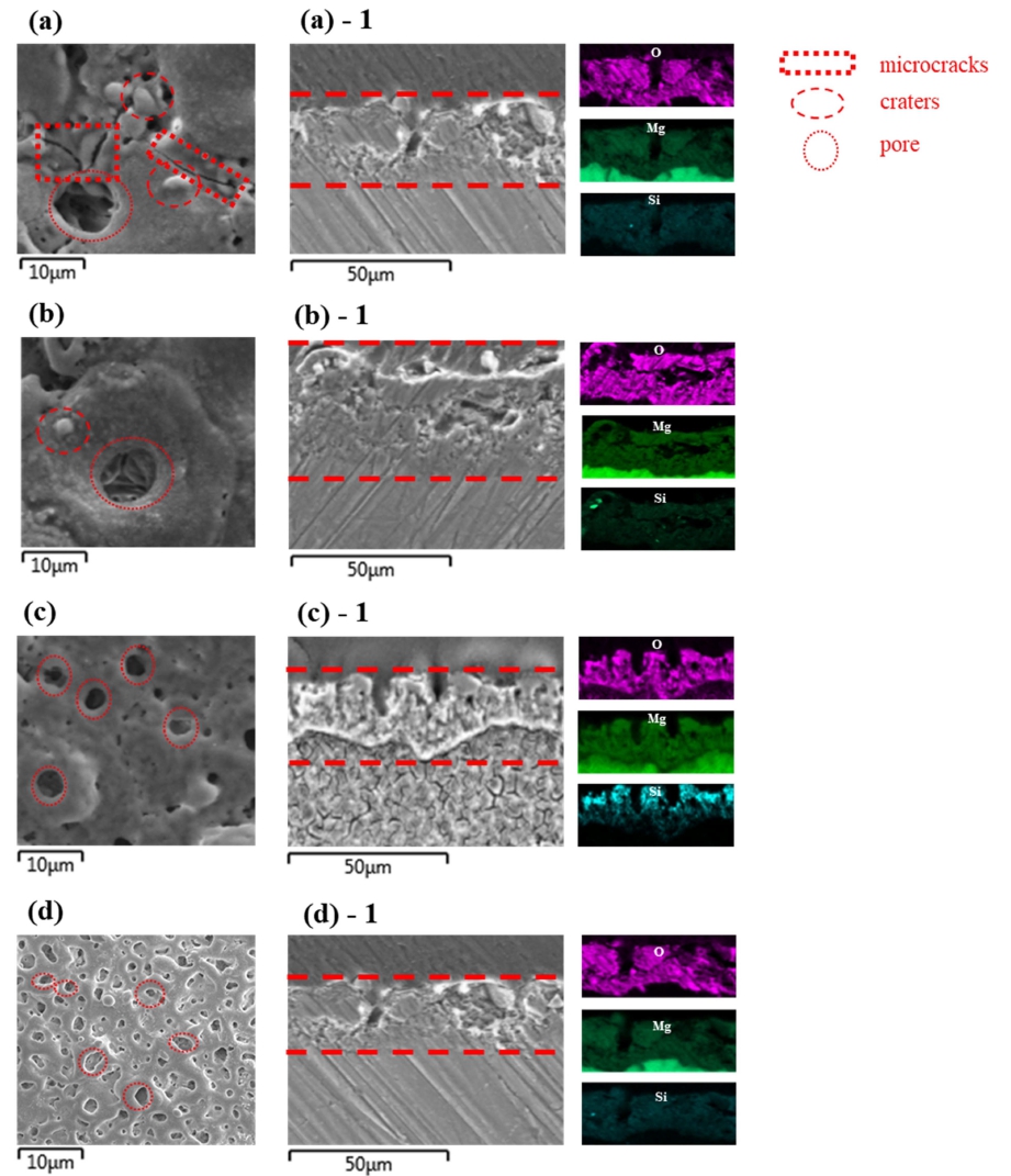
Fig. 1
Surface and cross-section morphologies and EDS element mapping of the AZ91D after plasma anodization at (a) 20 °C, (b) 30 °C, (c) 40 °C and (d) 50 °C.
The surface of the specimens treated at 20, and 30 °C showed uneven porosity and some microcracks and craters. The surface with cross section of oxidized specimens treated at 40 and 50 °C showed a relatively constant pore size.
The distribution of Mg, O and Si in oxide film uniformly distributed within the film at temperature.
Plasma anodic oxide films tend to be formed uniformly with decreasing thickness of the oxide film as the electrolyte temperature is increased.3)
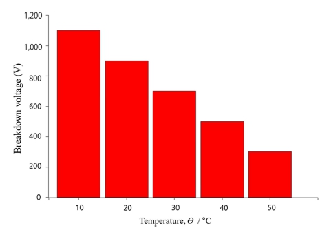
Figure 2 shows the results of dielectric breakdown voltage measurements for the plasma anodized AZ91D alloy in electrolytes with different temperatures. The dielectric breakdown field of MgO is about 10 MV/m.4) The specimen with plasma-anodized at 50 °C had an oxide film with mean thickness of 24 μm. The breakdown voltage of 280 V corresponds to the breakdown field of 13 MV/m which is close to the value of MgO. On the contrary, the breakdown voltage was as high as 1,080 V for the plasma anodized specimen's at 10 °C, with oxide layer of about 40 μm, The breakdown field of the oxide layer was doubled to 26 MV/m as compared with firm form at 50 °C.3) These results may be attributed to the oxide film formed at 10 °C having large pore and voids results in many micro cracks dispersed electricity.
Heat conducting property of the plasma anodized AZ91D was evaluated by the laser flash method. In this test, a laser energy pulse was applied to the AZ91D surface and the temperature change at the oxide surface was followed as shown in Fig. 3. The temperature change is typically characterized by the half time t1/2 in Fig. 3, from which thermal diffusivity can be calculated according to the Parker formula:
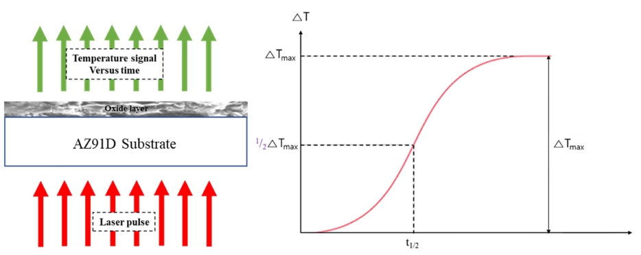
where α is thermal diffusivity (mm2 K−1) and d is the thickness of sample.
In the case of AZ91D without anodized oxide layer, t1/2 was 0.048 s giving the α value of 36 mm2 K−1.
As shown in Fig. 4, t1/2 increased as the surface of AZ91D was covered with oxide film. The largest value of t1/2 was observed for the specimen plasma anodized at 10 °C. There seems to be a correlation between the breakdown voltage and t1/2; as the oxide layer becomes thinner or denser, the layer becomes less resistant against electric or thermal gradient.
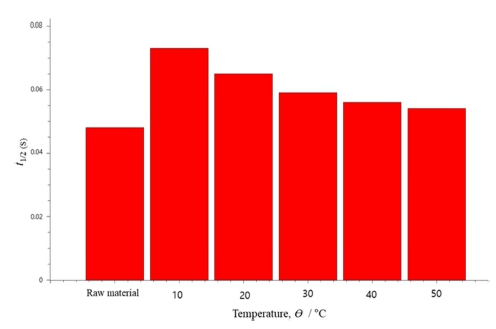
Fig. 4
Half time (t1/2) determined from the laser flash method for the AZ91D after plasma anodization in the electrolyte of different temperatures.
Although it is difficult to derive the thermal diffusivity value of oxide layer from this experiment, pure MgO is known to have relativity high thermal diffusivity of 19 mm2 s−1.4) Thermal conductivity of MgO as calculated by the following equation14,15) is 59 W m−1K−1:
where λ (Wm−1K−1) is the thermal conductivity, ρ (g/ cm3) is the density and Cp (J/kg · K) is the specific heat. On the other hand, the thermal conductivity of AZ91D as calculated from α = 36 mm2 K−1, ρ = 1.65 gcm−3 and Cp = 0.90 Jg-1K-1 is 53 Wm−1K−1. This value shows a good agreement with the reported value of 51.2 W m−1K−1.17) Thus, the thermal conductivity such as AZ91D is almost one-third of the pure magnesium (160 W m−1K−1) because of the introduction of alloying element of Al, Zn and Mn.
The experimental results of increased t1/2 by the plasma anodization indicates that the thermal conductivity of plasma anodizing oxide layer is somewhat lower than value of the raw material. A thermal conductivity value of about 8 Wm−1K−1 was reported for the plasma anodizing oxide layer on the Mg alloy material.18,19)
Plasma anodizing oxide film acts as a thermal barrier and the thickness of the oxide film and thermal conductivity are inversely proportional to each other. Thermal resistivity of the anodized AZ91D (R) is expressed as:
where L1 and L2 are the thickness of mother alloy and oxide layer, whereas λ1 and λ2 are the thermal conductivities of mother alloy and oxide layer, respectively. The thicker and less dense nature of the oxide layer formed at lower temperature is thus disadvantageous for heat conducting property. The apparent thermal resistivity of a 3 mm thick plate of AZ91D would increase by 5 % with plasma anodization at 50 °C assuming L1, λ1= 53 W m−1K−1 L2 = 24 μm and λ2 = 8 W m−1K−1.
Figure 5 shows the surface hardness of the AZ91D plasma anodized at different temperatures of electrolyte. The surface hardness of the AZ91D raw material was 80 Hv, while the plasma anodizing treatment at the electrolyte temperatures of 10, 20, 30, 40 and 50 °C showed hardness of 422, 578, 580, 628 and 634 Hv, respectively. Compared to the AZ91D raw material, hardness increased 5-7 times by the plasma anodization.
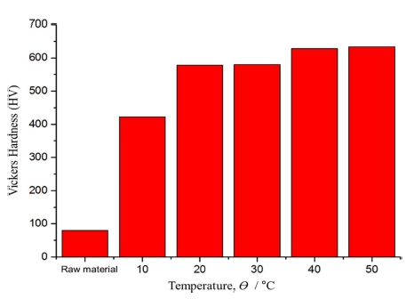
Fig. 5
Effect of electrolyte temperature on the Vickers hardness of the AZ91D after plasma anodization.
It is believed that the reason for the difference in hardness by the electrolyte temperature is the resulting difference in film density depending on the growth rate of the film at different temperatures.
Figure 6 shows the results of the friction test under the condition of Table 2, in which the normal load was 50 (a), 10 (b) and 1 N (c), respectively.
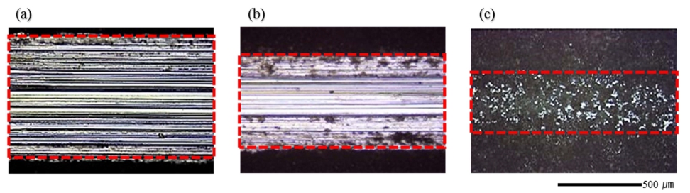
Fig. 6
Digital microscope surface photograph of AZ91D magnesium alloy after surface friction test specimens were plasma anodized by pulsed voltage of 150 V for 15 min at 50 °C (a) 50 N, (b) 10 N and (c) 1 N.
As a result of the tests, at the normal loads of 50 and 10 N, the oxide film on the surface of the specimen was completely removed with the track width of 750 μm. The center of the upper ball (SUJ2 steel, Ø 10 mm, 810 Hv) is estimated to have sinked in to into AZ91D (80 Hv) by 14 μm. At the normal load of 10 N, the bare track width became 580 μm corresponding to the maximum depth of 8 μm.
At the normal load of 1 N, oxide film remained on the surface after the test and the wear width was about 350 μm.
In order to evaluate the mechanical property of the oxide layer formed at different temperature, a normal load of 1 N was set under the condition of Table 2.
Figure 7 shows the result of friction test for the plasma anodized AZ91D at 20, 30, 40, and 50 °C.
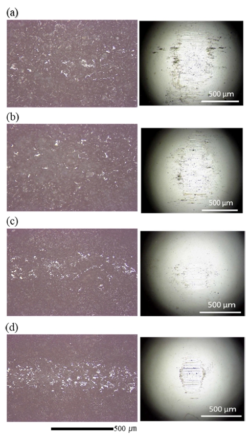
Fig. 7
Digital microscope surface photographs of AZ91D and SUJ2 steel ball after surface friction test friction test with plasma plasma anodization of AZ91D at (a) 20 °C, (b) 30 °C, (c) 40 °C and (d) 50 °C.
The results of showed that the worn width was about 850 μm for the films formed at 20 and 30 °C. In the case of films formed at 40 and 50 °C, the wear scar was about 350 μm in width.
This result is due to the higher surface hardness at the electrolyte temperature of 40, 50 °C, as shown in Fig. 5. As shown in the previous research,3) the surface roughness at 40, 50 °C was much smoother with less defects.
Figure 8 shows SEM images of the films formed at 20 and 50 °C after the friction test. There is no pore shape in the film formed 20 °C after the friction test. On the other hand, the film formed at 50 °C, had a pore shape which was crashed after the friction test. These results are related to the hardness of the surface.
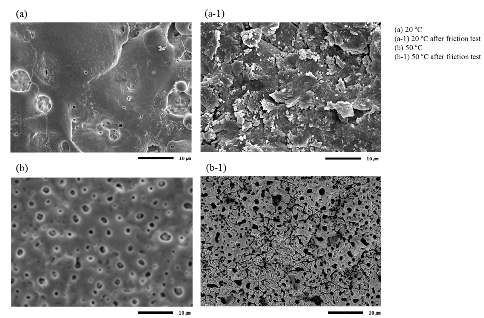
Fig. 8
Surface comparison before and after AZ91D surface friction test after plasma anodization at (a) out of track, (b) within track.
The oxide layer formed at 20 °C is relatively soft and easy to be deformed a contact with the steel ball. This why a wide but shallow scar formed as show in Fig. 7(a). The oxide layer formed at 50 °C is rather hard and deformed area is limited to cause a narrow but deeper scar as show in Fig. 7(d). It was confirmed that the oxide film was crushed by the friction test friction test.
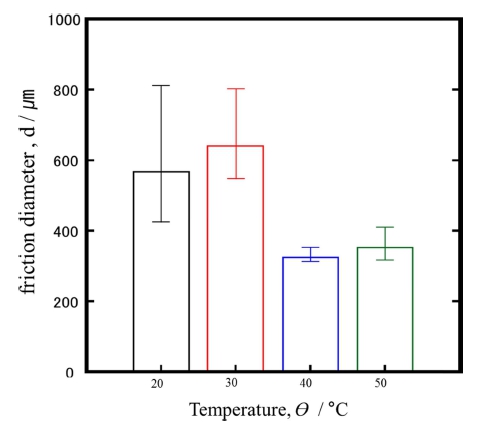
It is apparent that the scar width decreases with increase of electrolyte temperature for plasma anodization as summarized in Fig. 9. The above results are consistent with the results in Fig. 7.
4. Conclusion
In this chapter. the physical and mechanical properties of AZ91D magnesium alloy were evaluated as a function of electrolyte temperature for plasma anodization. As the temperature of the electrolyte increased from 10 °C to 50 °C, the breakdown voltage decreased because the formed oxide layer became thinner with less defect at high temperature. The oxide layer formed by the plasma anodization was evaluated for blocking heat conducting property of AZ91D by a laser flash method. The results indicated that heat resistivity became smaller as the electrolyte temperature increased because because of decrease breakdown voltage. With increase of electrolyte temperature. The Surface hardness increased, and the wear amount of the oxide film decreased as a result of the friction test. As temperature of the of the electrolyte increases, the surface hardness increases, the surface and cross-sectional defects decrease, the density decreases, and the surface roughness decreases. Based on the results of this study, the higher the temperature of the electrolyte, the better the anodic oxidation of AZ91D results in better physical physical and mechanical properties.
