

1. Introduction
Owing to the recent developments of electronic devices and electric vehicles, the demand for miniaturized, highly integrated, and high-performance components had increased considerably. As the heat generated during the use of electronic devices causes integrated circuit failure, heat spreading has become an attractive research topic. Moreover, even though the amount of heat generated during the use of electronic devices is not significant, heat damage can accumulate, shortening device life and deteriorating device stability. Hence, researchers should develop heat spreaders to mitigate this shortcoming.1) Heat spreaders include heatsinks, cooling fans, and heat spreadsheets. Heatsinks absorb heat directly and indirectly from products and then releases it. Cooling fans lower the temperature of products using air motion. Heat spreadsheets are used in lightweight or mobile products. Recently, increasing attention has been focused on carbonbased heat spread sheets.
Liu et al.2) mixed 2 wt% graphene and 2 wt% graphite sheet composites with paraffin, and reported that the thermal conductivities of the mixtures were 58.6 % and 41.4 % higher, respectively, than that of pure paraffin. Furthermore, Cu, Al, and Ag are primarily used as substrates for heat spreaders, and their thermal conductivities are 386, 239, and 419 W/(m·K), respectively.3) Recently, studies have been conducted on changing the microstructures of the existing heat spreaders or creating new heat spreaders by combining the existing ones. Yeo et al.4) increased the thermal conductivity of Al by 13 % by changing its microstructure. Park et al.5) demonstrated that the thermal diffusivities of Cu and Ag nanoparticle powders increased by approximately 10 % when the nanoparticles were mixed and coated. These studies developed effective heat spreaders by combining materials with high thermal conductivity. Therefore, it is expected that incorporating diamond, which is the material with the highest known thermal conductivity, into heat spreaders, their properties can be improved.
Single-crystalline diamond presents excellent thermal properties, such as a thermal conductivity of 2200 W/ (m·K) and a specific heat capacity of 0.54 J·g/K.6) Recent advances have allowed the fabrication of diamond thin films via chemical vapor deposition (CVD); therefore, researchers have focused their attention on developing heat spreaders using diamond thin films. The conventional thermal conductivity analysis method, which is typically used for investigating bulk samples, does not yield accurate results for thin films. Consequently, the development of a new measurement method that can precisely measure the thermal conductivity of thin films is critical.
Conventional thermal conductivity measurement methods include heat flow measurement (HFM), the 3-ω method, laser flashing analysis (LFA), and LaserPIT-M2 instruments. HFM method is not suitable for thin film samples because of their low measurement range; moreover, thermal conductivity is measured via heat transfer from the heat source to a heatsink. The 3-ω method, which is often used for thin film samples, involves applying a metal line heater and sensor simultaneously through fourpoint probe. The thermal conductivity is determined using the changes in voltage induced by the changes in temperature at the sample surface. Although the 3-ω method is accurate for insulating thin films and materials with low thermal conductivity, it is not suitable for thin films of high thermal conductivity.7) LFA can be used to measure the thermal conductivity in the horizontal direction. However, it is prone to errors when it is used to measure the thermal conductivity of heated thin film samples in the vertical direction. LaserPIT-M2 devices can be used to simultaneously measure the thermal conductivity of thin films and their substrates. Nevertheless, the practical use of LaserPIT-M2 instruments is hindered by their sample preparation specificity, which requires that thin films be grown only on half of the surface area of a rectangular substrate.
To overcome these shortcomings, in this study, we used the light source thermal analysis (LSTA) method for thermal conductivity measurements. LSTA measurements involve irradiating samples with heat from a light source and analyzing the changes in temperature at the sample surface. Therefore, the thermal conductivity of thin films can be easily determined by calibrating the heat from the heat source through measuring the temperatures of the substrate and substrate/thin film samples.
In this study we measured the thermal conductivity of polycrystalline diamond (PCD), which was uniformly grown into a 1.8 μm thick film using LSTA. Subsequently, the results were compared with those obtained using the representative conventional thermal conductivity measurement methods, namely LFA and LaserPIT-M2, to assess the potential of the newly proposed LSTA method.
2. Experimental Procedure
In this study, thin films were prepared by depositing PCD on a Si wafer using the hot-filament chemical vapor deposition (HFCVD) method. The CVD pretreatment consisted of a sequence of pre-cleaning, seeding, and cleaning steps. The thin film samples subjected to thermal conductivity measurement experiments using the three aforementioned methods were fabricated under the same experimental conditions.8,9)
The surface and cross-section microstructures of the prepared samples were analyzed using an optical microscope (AX-10, Zeiss) and a field emission scanning electron microscopy (FE-SEM; S-4300, Hitachi) instrument. The phase of the deposited PCD were evaluated using a micro-Raman spectrometer (UniRaman, UniThink) in the single mode utilizing a 532 nm laser.
Fig. 1 presents the schematic of the experimental setup employed for measuring the in-plane thermal conductivity using an LFA instrument (LFA447, Netzch). For the inplane thermal conductivity measurements, the front of the sample was exposed to heat radiation; however, the temperature of the back of the sample was measured through the slit at a certain distance from the holder center. The in-plane thermal diffusivity was measured using the measured temperature and the embedded software.10) Thereafter, the thermal conductivity (λ) of the sample was calculated as follows:
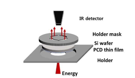
where α is the thermal diffusivity [m2/s] and Cρ is the volumetric heat capacity [J/(m3·K)].
Fig. 2 presents the schematic of the measurement setup using a LaserPIT-M2 (ULVAC-RIKO Inc.) device. The LaserPIT-M2 device can be utilized to measure the inplane thermal conductivity of thin films using the Angstrom method, which is an AC method.11) The LaserPIT-M2 device comprised a heat source, a main unit for mounting the sample, a vacuum pump, and a computer for calculations. A laser diode with a wavelength of 690 nm, an output of 30 mW, and a frequency of 10 Hz was used as the heat source. During the measurements, a vacuum of 0.02 Pa was created using a vacuum pump. To evaluate the thermal response characteristics of the samples, an E-type thermocouple (TC) was used. The thermal conductivity (λ) of thin film layers was determined using the difference in thermal diffusivity between the bare substrate and the area of the substrate covered with the thin film [12]. Consequently, the λ values of thin film layers can be calculated as follows:
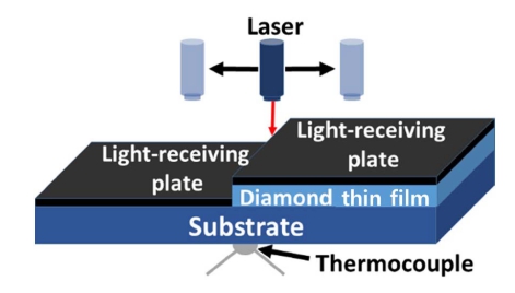
where α01 is the thermal diffusivity of the substrate [m2/ s], α012 is the thermal diffusivity of the thin-film-covered substrate [m2/s], α2 is the thermal diffusivity of the thin film layer [m2/s], C1 is the volumetric heat capacity of the substrate [J/(m3·K)], C2 is the volumetric heat capacity of the thin film [J/(m3·K)], d1 is the thickness of the substrate [m], and d2 is the thickness of the thin film [m].
Fig. 3(a) illustrates the LSTA measuring device, which was fabricated using a 3D printer. The device comprised a UV light source on the left and a temperature measuring unit on the right. Fig. 3(b) presents the schematic of the measuring device. The thermal conductivity measurements using this method were performed as follows. Two types of samples were subjected to measurements: Si(100) wafers and Si(100)/PCD specimens. The UV light source with a power of 4.8 W (Prime-100, Skycares) served as the heat source, and the sample was secured using a prefabricated jig at a predetermined height in respect to the heat source. This was intended to control the heat that escaped through the area of the device that came in contact with the sample upon activating the heat source. The surface temperature was measured using a TC. A thermal interface material (TIM; TFX thermal paste, Thermalright) was placed between the TC and the PCD thin film to lower the thermal contact resistance ascribed to the surface roughness of the PCD thin film. Thereafter, the heat source was activated and the changes in temperature were measured over 1,500 s using a data logger thermometer (GL240-UM-151, Graphtech).
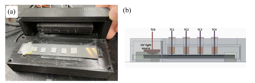
Fig. 3
LSTA device used for measuring thermal conductivity in this study: (a) photograph and (b) schematic.
Subsequently, the amount of heat in each layer of the uniform thin film was calculated as follows:
where, Qfilm is the amount of heat transmitted to the thin film layer [W], Qtot is the amount of heat applied to the entire sample [W], Cfilm is the heat capacity per unit volume of the thin film [J/(m3·K)], Csub is the heat capacity per unit volume of the substrate [J/(m3·K)], Vfilm is the volume of the thin film [m3], and Vsub is the volume of the substrate [m3].
The thermal conductivity of the thin film layers were obtained by substituting the amount of heat transmitted to the thin film (Qfilm) in the Fourier’s equation:
where Afilm is the surface area of the thin film in the heat transfer direction [m2], T is the temperature difference between the heat source and thermocouple [K], and x is the distance between the heat source and thermocouple [m].
The thermal conductivity of the Si(100) substrate with well-known physical properties was measured using the LSTA method, and the calibration factor was calculated by correcting the measured thermal conductivity of the Si(100) wafer. Thereafter the thermal conductivity of the Si(100)/PCD sample was measured using the LSTA method, and the final thermal conductivity of the PCD thin film was determined considering the aforementioned calibration factor of the Si(100) substrate.13)
3. Results and Discussion
Fig. 4 presents photographs of the HFCVD-prepared Si(100)/PCD samples subjected to thermal conductivity measurements using the LFA method, a LaserPIT-M2 instrument, and the LSTA method. The samples subjected to LFA were prepared by depositing PCD on 1'' Si(100) wafers [Fig. 4(a)]. The samples were disc-shaped to facilitate loading on the LFA equipment. The samples used for LaserPIT-M2 analysis were prepared by cutting a 4'' Si wafer into 30 mm × 2.5 - 5 mm rectangles and depositing PCD on half of their surfaces using a mask [Fig. 4(b)]. The LSTA sample was prepared by cutting a 4'' Si wafer into a 80 mm × 15 mm rectangle, followed by PCD on its entire surface [Fig. 4(c)]. The LSTA sample was easily prepared as it did not require shaping into a disk or masking.
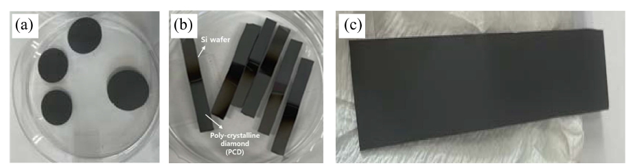
Fig. 4
Photographs of the HFCVD-prepared Si(100)/PCD samples for (a) LFA, (b) LaserPIT-M2, and (c) LSTA measurements.
The optical microscopy image of the sample surface, FE-SEM image of the sample revealing its surface microstructure, and FE-SEM cross-sectional image of the prepared 4'' Si(100)/PCD sample are presented in Fig. 5(a), (b), and (c), respectively. The 4'' Si(100)/PCD sample presented a uniform surface [Fig. 5(a)]. Moreover, the mean grain size of the PCD thin film was approximately 1 μm [Fig. 5(b)]. The thickness of the PCD thin film was approximately 1.8 μm [Fig. 5(c)]. Considering the HFCVD process time, we concluded that the PCD crystal grew at the rate of 0.36 μm/h.
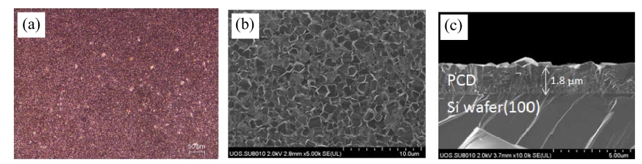
Fig. 5
Surface and cross-sectional images of a 4'' Si(100)/PCD sample: (a) Optical microscopy surface image, (b) FE-SEM surface image, and (c) FE-SEM cross-sectional image.
Fig. 6 illustrates the Raman spectrum of the Si(100)/ PCD sample, which includes Si and diamond peaks at 520 and 1,335 cm−1, respectively. The Si peak was detected despite the presence of the PCD thin film coated on the top surface of the Si wafer. This was attributed to the transparency of the micro-thick PCD film. Furthermore, a Si/SiO2 peak was observed at 900 cm−1, which was ascribed to the SiO2 layer on the surface of the Si substrate. Therefore, the Raman analysis results confirmed the diamond phase of the PCD thin film on the Si substrate using the HFCVD method.14,15)
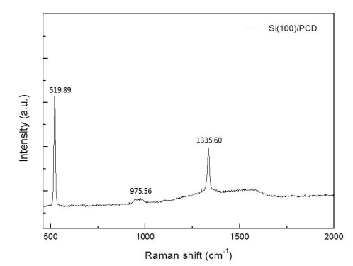
Table 1 summarizes the in-plane thermal conductivity values measured via LFA. The experiments were performed in triplicate and the average thermal conductivity of the sample was 1.706 W/(m·K). This was a significantly smaller value than the known thermal conductivity of diamond; moreover, this value was much smaller than the thermal conductivity of single-crystalline Si [140 W/(m·K)], which was used as the substrate.13)
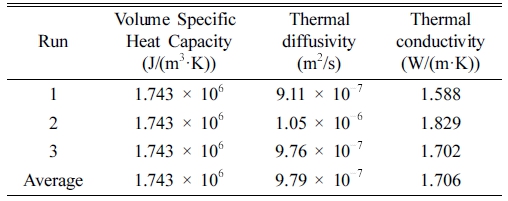
These results were attributed to a structural problem of the LFA equipment. The laser irradiates the front of the sample; however, the temperature is measured at the back of the sample. Consequently, the thermal conductivity is lower than the actual value because of noise, which can be attributed to the poor thermal contact between the substrate and thin film for thin film sample and the grain boundary of the PCD preventing heat transfer.16,17)
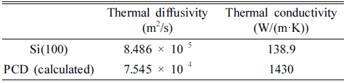
Table 2 presents the thermal conductivities of the substrate and thin films measured using a LaserPIT-M2 instrument. The thermal diffusivities of the Si(100) substrate and Si(100)/PCD areas of the samples were measured simultaneously, and were determined to be 8.486 × 10⁻⁵ and 7.545 10−4 m2/s, respectively. In addition, the corresponding thermal conductivities were 138.9 and 1430 W/(m·K), respectively. The measured thermal conductivity of the Si substrate was comparable with the reference value of 140 W/(m·K). However the measured thermal conductivity of the PCD thin film was significantly higher than the previously reported PCD thermal conductivity values, which ranged between 100 and 300 W/(m·K), and was comparable to that of single-crystalline diamond. Therefore, the thermal conductivities measured using the LaserPIT-M2 instrument were considered unreliable.18)
Table 2
Thermal diffusivities and conductivities of the Si(100) substrate and PCD thin film determined via LaserPIT-M2 analysis.
 |
The temperature–time curve used to determine the thermal conductivities of the Si substrate and Si(100)/ PCD samples using the LSTA method are presented in Fig. 7(a) and (b), respectively. The black line represents the time evolution of the temperature of TC0, which was located directly under the UV light source, and the red, blue, green, and fuchsia lines represent the time evolutions of the temperatures of TC1, TC2, TC3, and TC4, respectively as shown in Fig. 3(b). TC1, which was closest to the light source, presented the highest temperature among all the TCs after 1,500 s. This was attributed to the distance between TC1 and the light source being shorter than those between the other TCs and the light source, which minimized the heat loss through the surface. Consequently, the thermal conductivity of the PCD thin film was calculated using the data collected for TC1 to minimize the heat loss. For similar considerations, the thermal conductivity of the Si(100)/ PCD samples was calculated based on data collected for TC1.
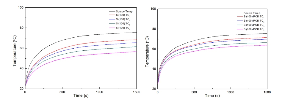
Table 3 summarizes the thermal conductivity data for the Si(100) wafer and Si(100)/PCD sample measured using the LSTA method. The thermal conductivity of the Si(100) wafer was calculated to be 846.56 W/(m·K) using a light power of 4.8 W. The calibration factor of 0.165 was determined based on the well-known thermal conductivity of the Si(100) wafer [140 W/(m·K)].
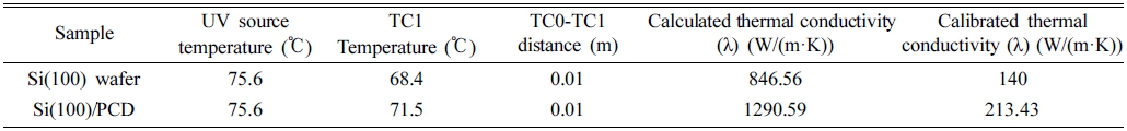
The LSTA-determined thermal conductivity of the Si(100)/PCD sample was 1290.59 W/(m·K). The thermal conductivity of the PCD thin film of the Si(100)/PCD sample was calculated to be 213.43 W/(m·K) by using the aforementioned calibration factor of Si substrate.
The calculated thermal conductivity of 213.43 W/ (m·K) of the PCD thin film with a PCD grain size of 1.8 μm was reliable considering that the thermal conductivities of PCD samples with grain sizes in the range of 0.5 - 2 μm reported by Cheng et al.18) and Angadi et al.19) ranged between 200 and 500 W/(m·K).
Therefore, the thermal conductivity of PCD thin film can be easily determined employing the newly proposed LSTA method by using an appropriate calibration factor.
4. Conclusion
First, 1.8 μm thick PCD films with a grain size of approximately 1 μm were deposited on single-crystal Si(100) substrates of various sizes using the HFCVD method. Thereafter, the thermal conductivities of the prepared Si(100)/PCD samples were measured using the LFA method, a LaserPIT-M2 instrument, and the proposed LSTA method. The results obtained using the LFA method and LaserPIT-M2 instrument were not accurate because the former underestimated and the latter overestimated the thermal conductivity of the PCD thin film. The newly proposed LSTA method enabled fast and reliable measurements based on a simple heat transfer process according to distance from the UV light source. The LSTA-determined thermal conductivity of the PCD thin film was 213.43 W/(m·K). This was similar to the values reported in previous studies for samples with similar grain sizes. Therefore, the LSTA method was the most appropriate thermal conductivity measurement method.
