

1. Introduction
Harvesting sunlight to provide clean chemical fuels such as hydrogen has been considered to be a desired and sustainable approach toward satisfying future energy demand with minimal adverse environmental impact.1,2,3) Various approaches have been attempted in order to develop some advanced processes for the production of hydrogen from the sunlight-driven splitting of water. Among those existing approaches, photoelectrochemical (PEC) water splitting is known to be one of the most promising hydrogen generation techniques in a highly efficient and eco-friendly way.4,5,6) In general, sunlight-driven water splitting process includes two half-cell reactions of the water oxidation or oxygen evolution reaction (OER) and the water reduction or hydrogen evolution reaction (HER). So the separation of water oxidation and reduction reactions is required for the process.7) Considering the fact that the PEC cells spatially separate HER and OER, those cells are widely used as sunlight-driven water splitting devices.
It is well known that the selection and design of the photocatalytic materials for the water oxidation photoelectrode or photoanode and water reduction photoelectrode or photocathode are crucial in a PEC cell system, since the capability of the PEC cell for water splitting is primarily determined by the light absorption and subsequent carrier transport in the photoelectrodes.8) So far, it has been identified that oxide semiconductors such as zinc oxide (ZnO), titanium dioxide (TiO2), hematite (Fe2O3), cupric oxide (CuO), and cuprous oxide (Cu2O) exhibit a promising potentiality as photoelectrodes for sunlight-driven hydrogen production.4,5,6,7,8,9,10,11,12,13,14,15) Among these oxide semiconductors, p-type CuO and Cu2O have been extensively investigated on their potential use as an efficient PEC photocathode for water reduction,4,5,6) since they exhibit several attractive features such as a bandgap adequate for absorbing the visible light, a sufficiently low toxicity, a significant earth-abundance, and a simple fabrication method.15) It has been reported that CuO and Cu2O have optical bandgaps of 1.3~2.1 eV and 2.1~2.6 eV, respectively,16) indicating that CuO has more potential for absorbing a vast majority of the sunlight spectrum. Moreover, the thermodynamic stability of CuO is known to be better than that of Cu2O. It is thus expected that CuO has a promising potentiality as a photocathodic material for an effective PEC water reduction.
Recently, it has been recognized that the PEC performance of photoelectrode based on an oxide semiconductor is strongly dependent on the dimension of the microstructure of the photocatalytic material.17) In this respect, CuO nanostructures including thin films, nanorods, and nanowires are considered to be much promising for a possible enhancement in the PEC performance owing to their large surface-to-volume ratios.18) Here we attempt to prepare very thin CuO thin films and vertically aligned CuO nanorods by a facile sputtering and hydrothermal synthesis methods, respectively.
In the present work, we report on the investigation of the comparative feasibility as an effective photocathode for PEC water reduction of CuO thin film and nanorod. Here, CuO thin film was prepared via a facile method combined with sputtering Cu metal film and subsequent thermal oxidation while CuO nanorod was synthesized via seed-mediated hydrothermal synthesis method with the use of a CuO nanoparticle seed layer. The structural, optical, and PEC properties of the prepared CuO thin film and nanorod were examined comparatively. Our results demonstrate that the CuO nanorod photocathod exhibits a higher photocurrent density and better photoconversion efficiency (PCE) than the CuO thin film photocathode for PEC water splitting, implying a promising route to the fabrication of CuO-based photoelectrodes.
2. Experimental Procedure
A CuO nanostructured thin film was prepared through two consecutive steps consisting of thermal oxidation of a sputtered Cu metal film in dry air.14) The Cu metal film was first deposited on a glass substrate coated with a fluorine-doped tin oxide (FTO) electrode from a pure Cu metal target by a rf sputtering method in an Ar atmosphere of 5 mTorr during 10 min at a sputtering power of 30 W. The substrate temperature was kept at room temperature and the substrate-to-target distance was set to be 12 cm. The as-sputtered Cu metal film was then thermally oxidized in dry air at a temperature of 400 °C for 1 h by using a rapid thermal annealing system with the increasing rate of the annealing temperature being kept at 10 °C/min.
A vertically aligned CuO nanorod array was prepared on a glass substrate coated with a FTO electrode via seed-mediated hydrothermal technique with the use of a CuO nanoparticle seed layer formed by a two-step method as previously described.19) The CuO nanoparticle seed layer, which acted as a nucleation layer for growing CuO nanorods, was formed using the same procedure as the procedure used for preparing the CuO thin film, with the sputtering of Cu metal being carried out for 2 min. The vertically-aligned CuO nanorod array was then synthesized by dipping the CuO-deposited substrate into a solution which consisted of 20 mM Cu(NO3)2 ‧ 3H2O and 40 mM C6H12N4 in distilled water, and by heating it at 90 °C for 3 h in an oven. Finally, the substrate covered with CuO nanorods was carefully cleaned with deionized (DI) water and dried under a high-purity nitrogen gas flow.
The microstructures of the prepared CuO thin films and nanorods were analyzed by scanning electron microscopy (SEM), and then their crystalline phases were characterized by X-ray diffraction (XRD) using Cu Kα radiation along with Raman spectroscopy. The optical properties of the prepared CuO thin films and nanorods were examined by UV-vis-NIR spectrometer. The CuO thin film and nanorod photocathodes were then fabricated by securing a Cu wire to the exposed electrically-conductive FTO substrate with Ag conducting paint and sealing the substrate on all edges with epoxy resin excepting the active working area. All the PEC measurements for the CuO thin film and nanorod photocathodes were performed in a three-electrode cell with the fabricated CuO photocathode as the working electrode, a Pt sheet as the counter electrode, and a Ag/AgCl as the reference electrode with an aqueous 1 mM Na2SO4 solution pH-adjusted to 6.6 as the electrolyte. The area of the fabricated photocathodes exposed to light were 0.5 × 1.0 cm2. The photoresponse was measured under a continuous irradiation from a 300 W Xe lamp, and the light intensity were calibrated to 1 mW/cm2 for the incidence onto the photocathodes.
3. Results and Discussion
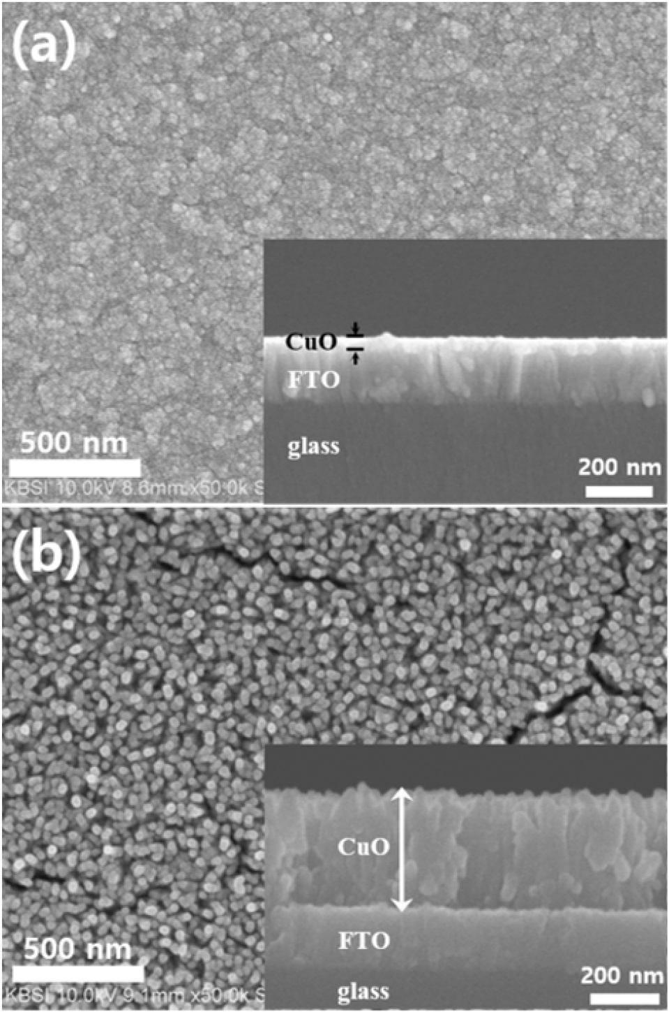
We present typical SEM images for the top-view and cross-sectional morphologies of the CuO thin film and nanorod array prepared on FTO-coated glass substrate in Fig. 1. Fig. 1(a, b) exhibit three obvious layers, that is, the bottom glass layer, the middle FTO electrode layer, and the top CuO layer. It is clearly seen from the SEM images in Fig. 1(a) that a dense CuO film as thin as ~40 nm with a columnar structure consisting of closely packed grains with sizes of the order of 10 nm is properly formed. The SEM images presented in Fig. 1(b) evidently indicate that vertically aligned CuO nanorods with average length and diameter estimated as ~400 nm and ~45 nm, respectively, are densely grown. The formation of the vertically aligned CuO nanorods can be explained by the relaxation mechanism of the stress induced by oxidation of Cu seed particles, where the only direction for relaxing the induced stress is known to be the vertical one.20) Also, the intensity of (110) and (111) facets of the vertically aligned CuO nanorods is found to be reduced compared to CuO thin film, which could be ascribed to the observed uniaxial vertical growth of the CuO nanorods. Given that the crystalline directionality of a semiconductor have an effect on the rate of the electron and/or transport, the uniaxial vertical growth of the CuO nanorods is possibly expected to be one of factors affecting the photoelectrode performance.
XRD was used to confirm the formation of the CuO crystalline phase. Fig. 2(a) shows typical XRD patterns of the CuO thin film and nanorod array prepared on FTO-coated glass substrate, indicating that the observed diffraction peaks with the exception of the peaks from the FTO layer for both CuO thin film and nanorod array simply correspond to the monoclinic tenorite CuO crystalline phase (JCPDS card no. 80-1268) and thus no diffraction peaks of second phases are detected here. The observed XRD results could suggest the successful preparation of the crystalline CuO thin film and nanorod array of the single phase.
The formation of the CuO crystalline phase could be further confirmed by the Raman spectroscopy analysis. Fig. 2(b) shows the Raman spectra of the CuO thin film and nanorod array prepared on FTO-coated glass substrates. In these observed spectra at room temperature, three distinct lines at around 280, 600, and 1,100 cm-1 can be ascribed to the characteristic phonon frequencies of the CuO crystalline phase.21) In consequence, both the observed XRD and Raman spectroscopy results demonstrate the successful preparation of the CuO thin film and nanorod array of the single phase.
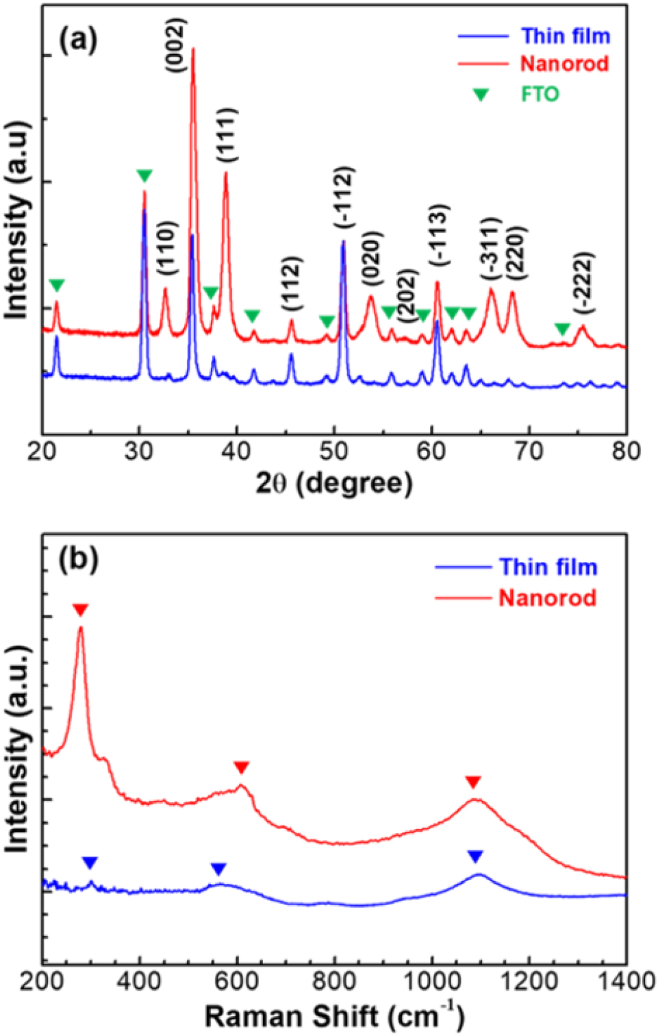
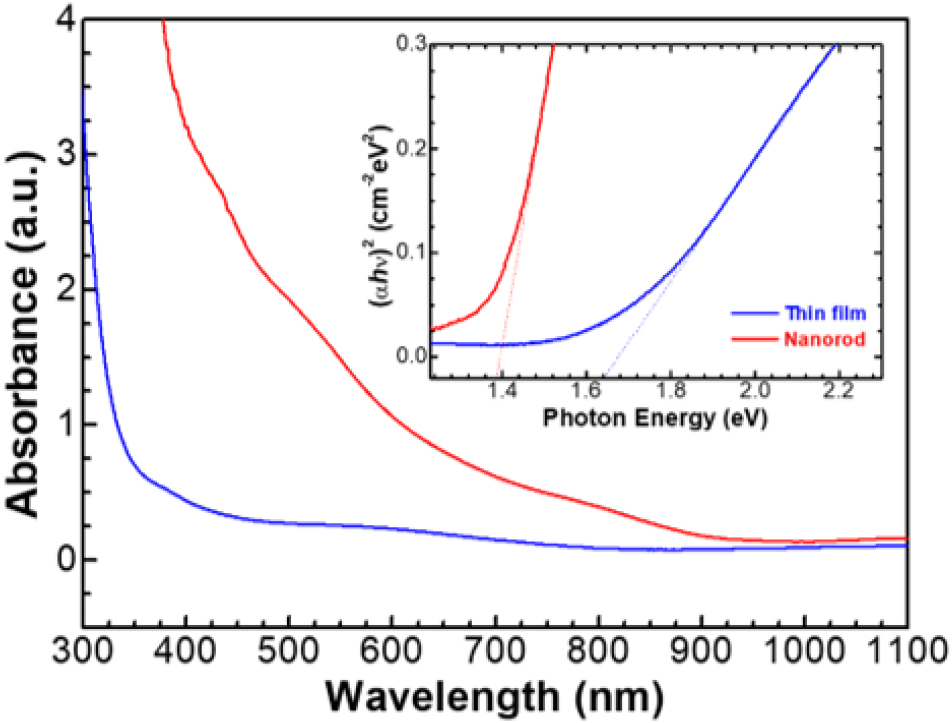
Fig. 3 shows the UV-vis-NIR absorbance spectra of the CuO thin film and nanorod array prepared on FTO-coated glass substrates. It is clearly seen from Fig. 3 that the prepared CuO thin film and nanorod array have absorption edges at about 900 nm due to the optical bandgap energy of CuO around 1.5 eV,16) indicating a significant potential for absorption of visible sunlight. Also, it is obviously found that the observed light absorbance of the CuO nanorod array is significantly higher than that of the CuO thin film, which is supposed to be partially related to the possible variation in the optical bandgap energy in accordance with the morphological variation of CuO.
The so-called Tauc plot, which is obtained from UV-vis-NIR spectrum, is generally used to determine the optical bandgap energy of semiconductor based on the following Eq. (1).22)
where, α is the absorption coefficient which can be obtained from the observed UV-vis-NIR spectrum, hν is the energy of photon, A is a constant, Eg is the optical bandgap energy, and exponent n is dependent on the nature of the optical transition. It is known that n is 2 for direct transition and n is 1/2 for indirect transition.23) As presented in the inset of Fig. 3, straight lines are obtained when (αhν)2 data are plotted against photon energy (hν), indicating that the optical absorptions for the CuO thin film and nanorod array are due to a direct transition. The estimated optical bandgap energies, which can be obtained from the intercepts on the abscissa, of the prepared CuO thin film and nanorod array are, respectively, 1.61 and 1.50 eV. These estimated optical bandgap energy values are in good agreement with the previous standard value of 1.5 eV for CuO.16) Also, as somewhat expected, the CuO nanorod array is found to exhibit the optical bandgap energy smaller than the CuO thin film, which give a partial explanation for the larger observed absorbance for the CuO nanorod array. It is known that the bandgap of semiconductor nanomaterials can be varied by their sizes and shapes,24) and thus the observed result of the bandgap of the CuO nanorod array being smaller than that of the CuO thin film could be principally related to the dimensionality reduction in the nanorod structure compared to the thin film structure. Here we should note that the observed bandgap difference in CuO thin film and nanorod structures gives rise to the difference in their optical absorbance, resulting in the difference in the rate of the photocatalytic reaction and consequently affecting the PCE of the CuO thin film and nanorod photocathodes.
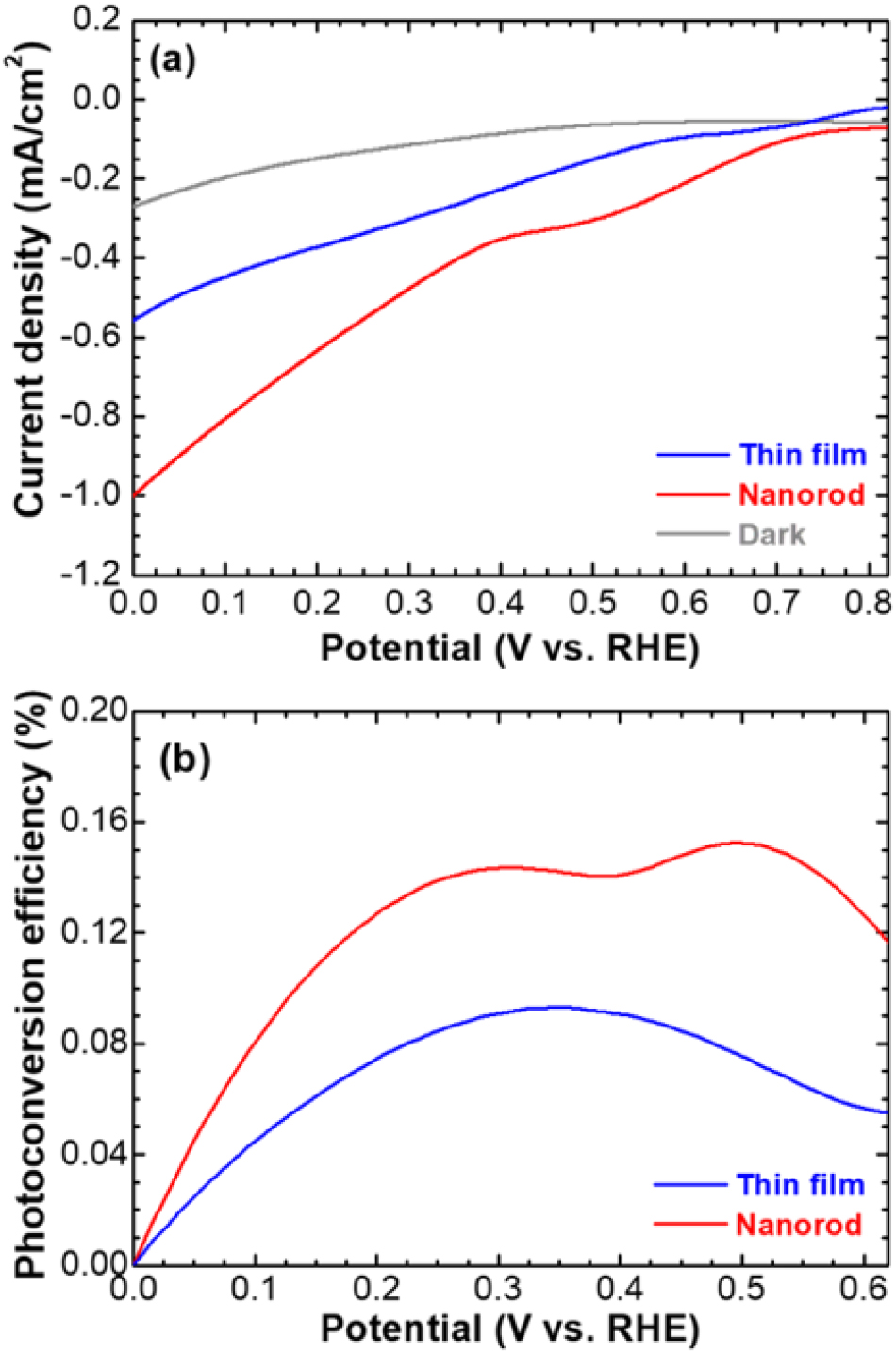
The PEC water reduction performances of the fabricated CuO thin film and nanorod photocathodes were characterized through the current density-potential (J-V) response curves measured using the linear sweep voltammetry under white light illumination. Fig. 4(a) shows the measured current density curves of the fabricated CuO thin film and nanorod photocathodes under the applied potential vs. the reversible hydrogen electrode (RHE), ERHE, which was derived according to the following Nernst relationship expressed by Eq. (2).25)
where, ERHE (V) is the converted potential vs. RHE, EAg/AgCl (V) is the external potential measured against the Ag/AgCl reference electrode, E0Ag/AgCl (V) is the standard electrode potential of the Ag/AgCl reference electrode (0.1976 V vs. RHE at 25 °C),8) and pH is the acidity of the solution. From the current density data of the CuO nanorod photocathode in the dark, the photoelectrode is clearly seen to exhibit quite insignificant photocurrent density, which is also the case for the CuO thin film photocathode. On the other hand, under light illumination, both the CuO thin film and nanorod photocathodes display a significantly enhanced cathode photocurrent density, which is mainly ascribed to the PEC water reduction. It is clearly seen from Fig. 4(a) that the CuO nanorod photocathode has the performance of PEC water reduction better than the CuO thin film photocathode. For example, the photocurrent density of the CuO nanorod photocathode is found to be -0.21 mA/cm2 at 0 V vs. Ag/AgCl (that is, 0.59 V vs. RHE), which is 2.3 times greater than that of the CuO thin film photocathode (-0.09 mA/cm2). The observed enhancement in the PEC water reduction performance for the CuO nanorod photocathode could be ascribed to an increase in the effective surface reaction area.
The PCE for PEC water reduction of the photocathode was estimated from our observed J-V characteristic data using the following Eq. (3).26)
where, ERHE (V) is the applied external potential vs. RHE, Jp (mA/cm2) is the measured current density at ERHE under light illumination, and Pi (mW/cm2) is the power density of the incident light. In Fig. 4(b) is presented the estimated PCE curves of the CuO thin film and nanorod photocathodes under an applied voltage vs. RHE. As expected from the observed PEC response characteristics in Fig. 4(a), the CuO nanorod photocathode has the PCE better than the CuO thin film photocathode. In consequence, it is revealed that the CuO nanorod photocathode exhibits the maximum PCE of 0.15 %, which is 1.7 times higher than that of 0.09 % for the CuO thin film photocathode, which is somewhat higher than that of 0.08 % for an electrodeposited nanostructured CuO thin film photocathode.15) Here we should note that the PCE of a photoelectrode is mainly determined by the product of the rate of the surface photocatalytic reaction and the rate of the carrier transport through the photocatalytic material. It is thus expected that the thickness of the CuO thin film and the length of the CuO nanorod have an effect on the PCE of the corresponding photocathodes, and it can be clearly seen that the thinner CuO thin film and the shorter CuO nanorod photocathodes have an enhanced rate of the carrier transport, possibly leading to an enhancement of the PCE. Considering the fact that the thickness of CuO thin film is ~40 nm while the vertically aligned CuO nanorods have an average length of ~400 nm, as shown in Fig. 1, our PEC results convincingly demonstrate that the CuO nanorod photocathode can possess the PEC performance better than CuO thin film photocathode due to the much greater rate of the surface photocatalytic reaction of the CuO nanorod than that of the CuO thin film.
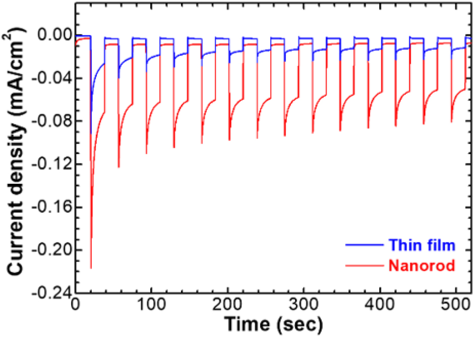
The long-term stabilities of the CuO thin film and nanorod photocathodes were examined by obtaining the current density-time (J-t) response curves under white light illumination. Fig. 5 shows the observed photocurrent responses of the CuO thin film and nanorod photocathodes at a bias voltage of 0 V vs. Ag/AgCl with light chopped (on/off) during each 20 s. It is seen from Fig. 5 that no significant photocurrent is in the dark. When the light was illuminated, the photocurrent has climbed promptly and then gradually reached a stable state, which is associated with the photogenerated electrons under white light radiation, the recombination of photogenerated electron-hole pairs, and the balance of generation and recombination of electron-hole pairs.13) As shown in Fig. 5, the CuO nanorod photocathode features a higher photocurrent density than that of the CuO thin film photocathode while the photostability of the CuO nanorod photocathode degrades as rapidly as the photostability of the CuO thin film photocathode. The photocurrent density for the CuO nanorod photocathode is found to be stabilized after ~4 min with the stabilized magnitude of the photocurrent density being ~67 % of the initial magnitude, which suggesting its long-term stability to be addressed.
4. Conclusion
In summary, a CuO very thin film was prepared via a facile method combined with sputtering Cu metal film and subsequent thermal oxidation while a vertically-aligned CuO nanorod array was grown via seed-mediated hydrothermal synthesis method with the use of a CuO nanoparticle seed layer. The observed XRD patterns and Raman spectra confirmed the formation of the monoclinic CuO single phase in both the CuO thin film and nanorod array. The PEC characteristics of the CuO nanorod photocathode are found to be superior to those of the CuO thin film photocathode due to the benefits specific to the nanorod morphology, that is, the increased effective surface area and the improved visble-light absorbance. The results of this work suggest that the vertically-aligned CuO nanorod array has promising potential as an effective photocathode for PEC water splitting.
