

1. Introduction
Perovskite alkaline-earth stannates ASnO3 (A = Ca, Sr, or Ba) have attracted more and more attentions as transparent conducting oxides (TCOs) with high electron mobility and transparency, which leads to promising applications in optoelectronic devices such as photovoltaic cells, wearable devices and flat panel displays (FPDs).1-3) These materials are believed to be the ideal replacement of the commonly used Sn doped In2O3 (ITO) TCOs, owing to their advantages including abundant and inexpensive resources, thermal and chemical instability, low phonon scattering, and wide band gaps.4,5)
As a member of stannates, SrSnO3 (SSO) has a higher optical transparency in the visible and near-infrared bands and an ultra-wide bandgap in the range of 4~6 eV. Furthermore, SSO crystallizes in perovskite orthorhombic GdFeO3 structure with three-dimensional multi-twinning unit cells, and the lattice parameters are a = 5.709 Å, b = 5.703 Å, and c = 8.064 Å.6,7) The lattice parameter of pseudocubic SrSnO3 is apc = 4.037 Å (where the subscript indicates pseudocubic notation), which is compatible with many transparent oxide substrates, such as MgO, LaAlO3, and SrTiO3 crystals. The electrical and optical properties of Ta- and Nb-doped SSO epitaxial thin films grown on MgO and LaAlO3 substrates were reported.8,9) Wide-range band-gap engineering was achieved in SSO films with Pb- and La-ions dopants while maintaining high optical transmittance in the visible light region.10,11)
As is known, pure stoichiometric bulk SSO is a white insulator. However, defects will be inevitably produced during the preparation of low-dimensional materials. Oxygen vacancies (OVs) are the most prominent characteristics of perovskite oxide thin films due to the lack of oxygen.12) The existing OVs in SSO thin films can not only modify significantly the band gap width, but also perform as electron donors,13,14) which will turn SSO films into n-type semiconductors. In this paper, we describe the preparation of c-axis oriented epitaxial SSO thin films deposited on 1.0 wt% Nb-doped SrTiO3 (NSTO) single crystal substrates by using a pulsed laser deposition (PLD) technique. The temperature-dependent electrical transport properties of the epitaxial heterostructure were investigated.
2. Experiment
Epitaxial SSO thin films were deposited on NSTO (001) substrates by pulsed laser deposition using a Lambda Physic KrF excimer laser with a wavelength of 248 nm operating at 3 Hz repetition rate as energy source. High purity SrCO3 and SnO2 powders were used in a traditional solid-state process to create the ceramic SSO target. The raw materials were milled and then calcined at 1,200 °C for 10 h to achieve the necessary Sr and Sn stoichiometry. The fine powders were formed into a 20 mm diameter and 5 mm thickness disk and sintered for 12 h at a final temperature of 1,500 °C into a target.
A rotating holder with the SSO target fixed on it was 35 mm away from the NSTO substrates. A resistive heater was used to keep the substrates at 750 °C during the process of deposition. The chamber was pumped to a base vacuum level of 1.0 × 10⁻⁴ Pa by the combined using of mechanical and turbo-molecular pumps prior to the deposition. Then, the deposition was carried out under an oxygen pressure of 10 Pa, and the laser energy density on the target was about 2.5 J/cm2. The SSO film thickness was determined to be about 180 nm with an uncertainty of ±5 % by a surface profile measuring system.
Structural characterization and crystallographic orientation of the SSO film were analyzed by using x-ray diffraction (XRD) with a Cu Kα source (λ = 1.5418 Ǻ). In-plane and out-of-plane diffraction θ-2θ scans and φ scans were carried out to determine the phase purity and epitaxial nature at the interface. X-ray photoelectron spectroscopy (XPS) measurement was performed to check the composition and binding energy of the elements by using Mg Kα (hν = 1,253.6 eV) as the exciting radiation. The prepared samples were placed in a liquid nitrogen system, and the current-voltage (IV) measurements were performed by combined using of Keithley 2400 SourceMeter and LakeShore Model 322 Controller to show the temperature-dependent transport properties of the SSO/NSTO interface.
3. Results and Discussion
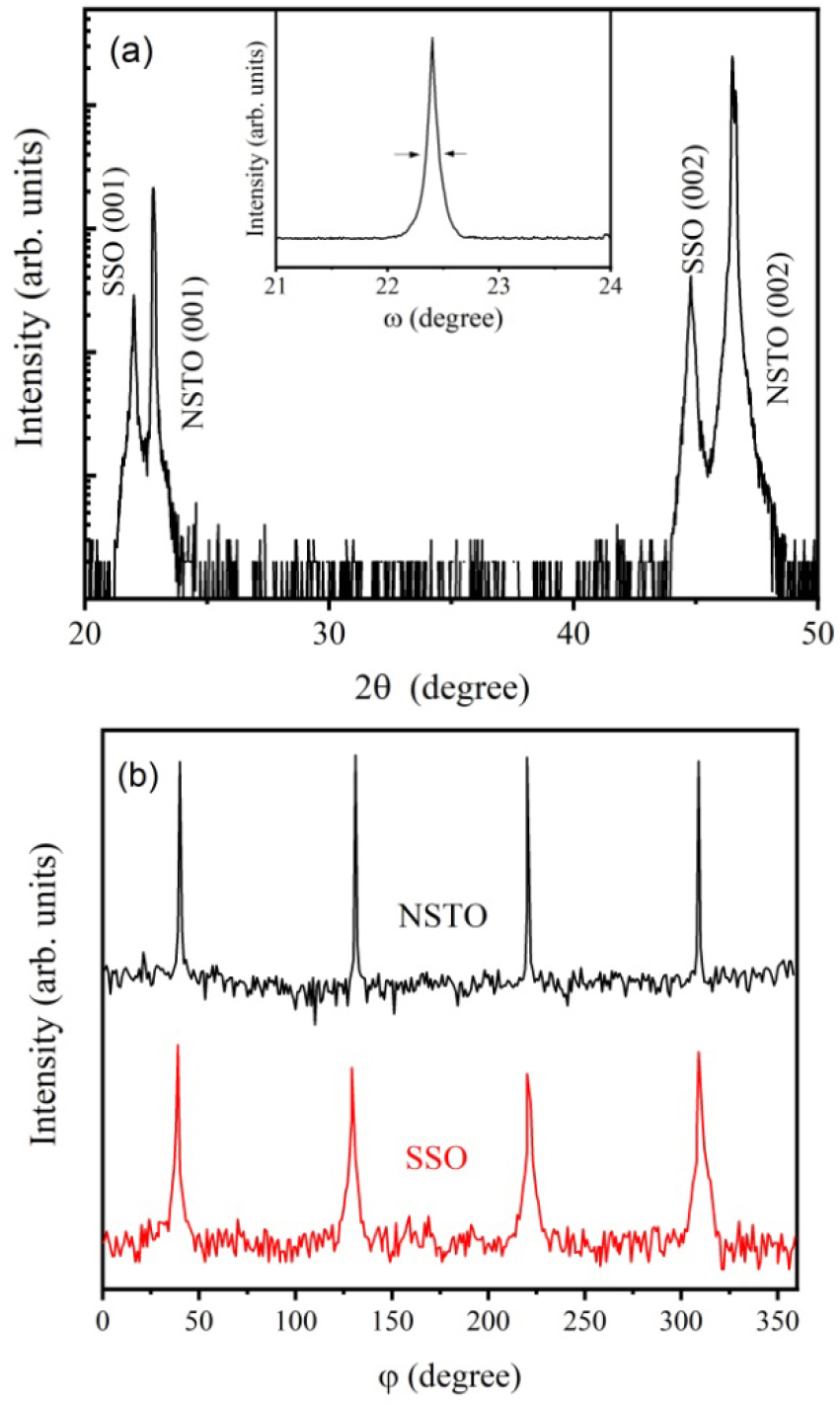
Fig. 1(a) shows an XRD profile of the SSO film grown on a NSTO (001) substrate. In addition to the strong diffraction peaks from substrate, only (00l) peaks for the SSO thin film are observed. No impurity phases or randomly oriented grain peaks can be detected, indicating that the prepared SSO film is single-phased and ideally c-axis oriented. The full width at half-maximum of the x-ray rocking curve from the (002) peak is about 0.21°, as shown in the inset of Fig. 1(a), suggesting the good crystallinity of the SSO film. The out-of-plane pseudocubic lattice parameter c of SSO film was calculated to be 4.082 Å, a little larger than that of SSO bulk.15)
X-ray φ scans around the SSO (101) and NSTO (112) peaks were carried out to investigate the in-plane texture of the SSO/NSTO heterostructure. As shown in Fig. 1(b), the pattern of SSO displays a clear four-fold symmetry with 90° intervals that coincides with the underlying NSTO substrate. As is well known, the lattice parameter of cubic-structured NSTO is a(b) = 3.905 Å, while that of SSO in pseudocubic structure is a(b)pc = 4.037 Å. The mismatches may result in appearance of compressive stresses in the ab plane of SSO film, which is responsible for the increased value of lattice c. The in-plane relationship between the SSO film and the NSTO substrate was supposed in a cube-on-cube epitaxial growth mode.
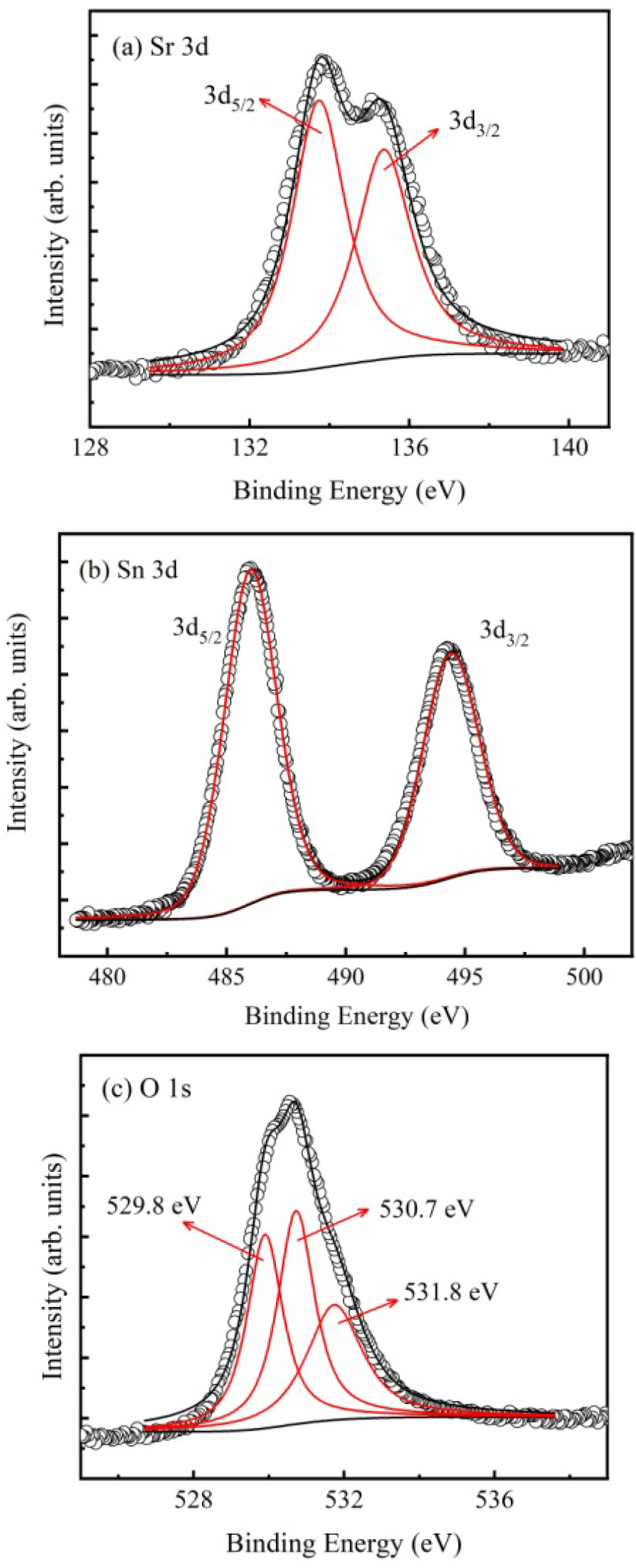
XPS spectra were used to examine the chemical state and concentration of the components in the fabricated SSO film. The data were calibrated with the assumed value of 284.8 eV for the C 1s binding energy. The Sr 3d spectrum with a 1.8 eV peak separation is shown in Fig. 2(a). Two peaks centered at 133.6 eV (Sr 3d5/2) and 135.4 eV (Sr 3d3/2) can be used to fit the data, indicating the Sr2+ oxidation state in the film. XPS region scan for Sn 3d is shown in Fig. 2(b). The Sn 3d5/2 and 3d3/2 core level binding energies are located at 486.27 and 494.68 eV, respectively, showing the presence of Sn4+ ions in the SSO film. As shown in Fig. 2(c), the asymmetric O 1s spectrum can be resolved into three peaks. The peak centered at 529.8 eV can be attributed to the lattice oxygen of the film. The other two peaks located at 530.7 eV and 531.8 eV, respectively, are possibly due to the OVs and C-O or H-O adsorptions on the film surface.16,17)
Conventionally, bulk perovskite oxides are treated as insulators. However, the existing defects or oxygen vacancies will turn the oxide thin films into semiconductors. As is known, defects in the oxide thin films have strong dependence on the ambient oxygen pressure.18,19) In the process of PLD, the emergence of OVs seems inevitable under the lower deposition oxygen pressures. The OVs mechanism can be expressed as
The existing OVs can perform as electron donors,13,14) which may turn the deposited SSO film into n-type semiconductor. The component element concentration for the SSO film can be quantified by calculating the atomic ratio of Sr/Sn/O. By using the XPS data analysis software, value of this ratio is determined about 1:1:2.89, suggesting the chemical composition of SSO film.
For IV measurements, a gold pad (0.2 mm2) was ex situ sputtered on the SSO film as top electrode and the bottom electrode was In (1 mm2) pressed onto the NSTO substrate. The Au and In electrodes were used to reduce possible contact barrier. It has been reported that contact of Au/perovskite oxide films and In/NSTO is good Ohmic.20,21) The Au and In electrodes were used as ohmic contacts for SSO and NSTO, respectively. By applying a pulsed dc bias across the interface with the voltage polarity defined at the bottom In electrode, the temperature-dependent IV curves were measured. The scan direction is set from positive to negative voltage in the range of 2~-1.2 V with 0.02 V intervals. The sketch of the experimental setup is illustrated in the lower inset of Fig. 3.
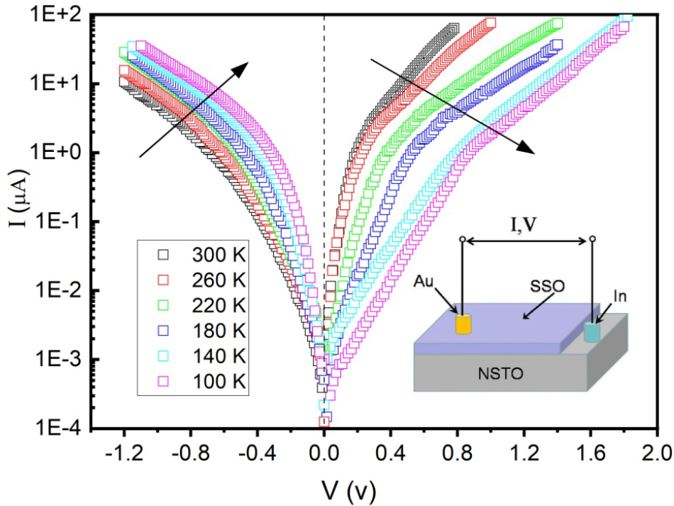
Fig. 3 shows the semilogarithmic temperature-dependent IV curves of the fabricated SSO/NSTO heterostructure. The diodelike rectifying behavior in the temperature range of 100~300 K indicates the junction characteristic. It is known that Nb-doped SrTiO3 is a degenerate n-type semiconductor, and highly doped NSTO substrate behaves as a metal phase.22) The as-prepared SSO/NSTO interface can be treated as a Schottky junction.
At positive bias, the current increase rapidly with increasing the applied voltage. When T is decreased from 300 K to 100 K, the diffusion voltage increases monotonically. The breakdown voltage, at which the current starts to grow at reverse bias, does not drop with decreasing T, as it does in ordinary Schottky junctions. The arrows in Fig. 3 indicate the trend in opposite direction. The increasing reverse-bias current at low temperature seems to make the semilogarithmic plot show a symmetric-like shape. The striking IV curves at reverse bias imply the tunneling effects at the temperatures investigated.
For a Schottky junction, the forward current can be described by the following equation,
where, Is is the saturation current, q, T, n, and kB are elementary charge, junction temperature, ideality factor, and Boltzman constant, respectively. V is the bias voltage applied across the junction. Fig. 4(a) shows the fitting plots of the forward IV curves, and two regions with different slopes can be detected. The boundary line (the black dash line) can be expressed by the equation,
Although the rectifying behavior has been observed in all-oxide rare earth manganites TbMnO3/Nb-SrTiO3 or HoMnO3/Nb-SrTiO3 structures,23,24) the IV curves separated into two regions by a curve are reported for the first time.
The diode ideality factor can be calculated from the slopes of the linear parts of the forward semilogarithmic plots. In region I, the extracted n increases from 1.0 to 2.0 with the decreasing temperatures, which means the dominant current transport mechanism is changing from diffusion to recombination.25) In region II, the obtained value of n is greater than 2 and the current transport mechanism can be attributed to the deep-level-assisted tunneling mechanism.26,27) Temperature dependency of n in two regions bounded by Eq. (3) is shown in Fig. 4(b).

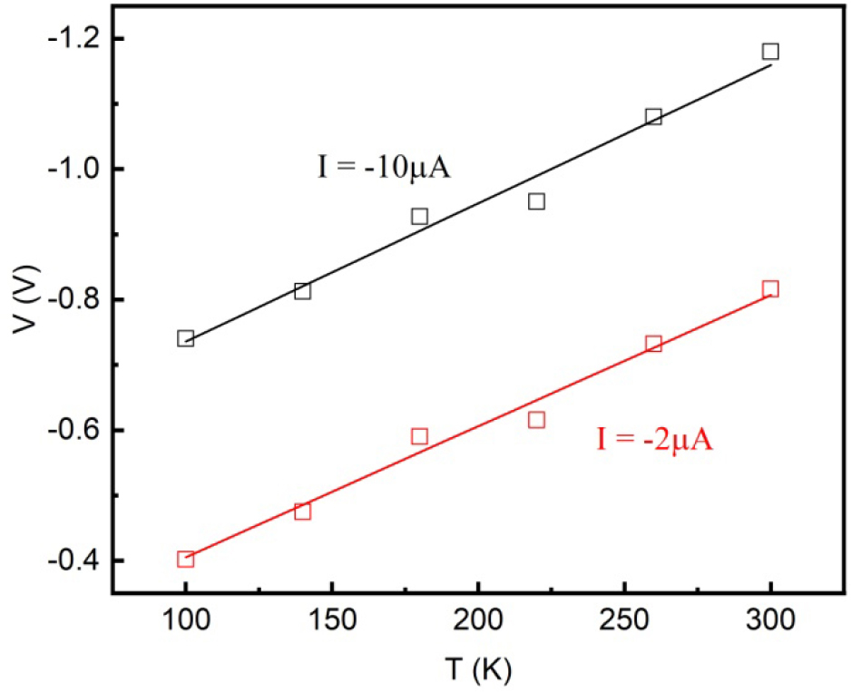
As the temperature is reduced from 300 to 100 K, the junction’s leakage current increases at a given reverse bias. Obviously, the thermionic emission cannot account for this unusual behavior. In the case of tunneling mechanism, the bias voltages at different temperatures for reaching a given tunneling current should satisfy the linear relation V-αkBT = constant, where αkB is measured in electron volts, that is, kB = 8.63 × 10⁻⁵ eV/K, and α is a fitting constant.28)Fig. 5 shows the voltages for reaching -2 µA and -10 µA reverse currents and confirms the linear dependence on T. The fittings to the data yield α = 23.2 for -2 µA and α = 24.5 for -10 µA. The values are comparable with that reported values for all-perovskite oxide PZT/NSTO junctions.28)
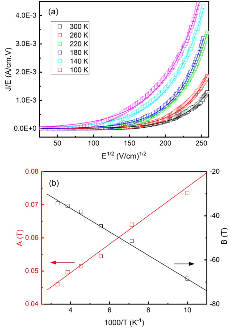
In general, Poole-Frenkel emission, hopping conduction, ohmic conduction, space-charge- limited conduction, and ionic conduction are typical examples of the bulk-limited conduction mechanisms. For Poole-Frenkel emission mechanism, the current density J is given by29)
where, E is the electric field at the interface, A(T) and B(T) are functions of T, can be characterized by
and
where, q the electronic charge, π, µ, and k are constants, e0 and es are the permittivity of free space and relative dielectric permittivity, respectively, j is the barrier height in eV.
Fig. 6(a) shows the conductivity (J/E) as a function of E1/2. The fitting results by using Eq. (4) were plotted as solid lines, and the agreement is satisfactory. The extracted values of A(T) and B(T) were also plotted as functions of 1/T, as shown in Fig. 6(b). As defined in Eqs. (5) and (6), the slope of A(T) vs 1/T yields es = 14, while that of B(T) vs 1/T yields j = 0.46 eV. The obtained value of es is in agreement with the reported relative dielectric permittivity of SSO.30) The barrier heights of junctions with similar structures in Refs. (31) and (32) (j = 0.41 eV for SrTiO3/La0.67Ca0.33MnO3, j = 0.40~0.48 eV for HoMnO3/Nb-SrTiO3) are comparable with our results. It is worth noting that different preparation conditions will cause the change of OV concentrations, which will affect the barrier heights of the junctions.
4. Conclusion
In summary, we have demonstrated perovskite single-phased SSO film grown epitaxially on NSTO substrate by using pulsed laser deposition. Under low oxygen pressure, the existing OVs change the prepared film into n-type semiconductor. The IV curves demonstrate diodelike rectifying behavior, indicating the junction characteristic of SSO/NSTO heterostructure. At positive bias, two regions with different transport mechanism were separated. The Poole-Frenkel emission mechanism was used to explain the increase of the reverse current with decreasing temperature.
