1. Introduction
Surface acoustic waves (SAWs) are an elastic wave that travels along the surface of a piezoelectric material and was first discovered by Rayleigh in 1885.1) The propagation phenomenon of SAWs was clarified by White and Voltmer, and the interdigital transducer (IDT) was first made in 1965.2) The IDTs consists of two interlocking comb-shaped metal electrodes deposited on a piezoelectric material. When a sinusoidal wave is applied to the SAW device, the piezoelectric material beneath the IDT vibrates due to the inverse piezoelectric effect, and at this time, the electrical energy is converted into acoustic energy, generating an acoustic wave perpendicular to the IDT.3,4) The SAW technology has been used in a wide range of applications, including wireless radio transmission5,6) [filters, spectral duplexers, radio frequency identification (RFID) tags], mesoscopic systems,7) and a variety of sensors such as chemical vapor,8) humidity,9) biology,10) gas,11) pressure,12) and contaminants.13)
In particular, microfluidic devices have attracted much attention in the field of biosensors. Due to their ability to precisely control very small amounts of samples and reagents, such as separation and mixing, these devices are excellent platforms for performing detection with high resolution and sensitivity.14) Recently, various technologies such as electrowetting, magnetics, and optics have been widely integrated into microfluidics to precisely manipulate fluids inside microchannels, which has led to significant progress in SAW technology.15)
In terms of electrode structure, SAW-based sensors typically consist of a pair of IDTs with opposite directions, one as the input IDT and the other as the output. The SAW velocity change between the input and output IDTs is characterized by phase shift and amplitude difference, which is expressed as an oscillating electrical signal of the output based on the inverse piezoelectric effect.16) The SAW sensors are composed of a single metal such as gold (Au) and aluminum (Al) on a LiNbO3 piezoelectric substrate. Au-IDT electrodes with a density of 19.3 g/cm3 have excellent electrical properties, but suppress the generation of vibration frequencies in SAW devices. On the other hand, the Al-IDT electrodes have low density, making it relatively easy to generate acoustic waves, but their poor electrical properties increase the resistance of the SAW devices. Therefore, to complement the shortcomings of these single IDT electrodes, the development of composite materials that simultaneously satisfy electrical and mechanical properties is necessary to improve the performance of SAW devices.
Typically, SAW-IDT electrodes are fabricated by two processes: electron beam (e-beam) evaporation and direct current / radio frequency (DC/RF) sputtering. Although the e-beam evaporation is optimized for growing various types of single metal thin films, problems such as phase changes may occur in the growth of multicomponent thin films due to the difference in melting points between materials. The DC/RF sputtering method can grow thin films without temperature limitations using various metallic or nonmetallic materials, making it suitable for implementing composite thin films with various physical properties. In particular, combinatorial sputtering can produce thin films with composition and thickness gradients in a one-pot process, making it very useful for exploring optimized materials.17,18)
In this study, we investigated the feasibility of utilizing Cu-Ti composite thin films as IDT electrodes to enhance the performance of SAW devices. Given the high electrical conductivity of Cu and the low density and excellent corrosion resistance of Ti, we aimed to optimize both the electrical and mechanical properties of SAW devices by combining these two metals. Cu-Ti thin films with various Cu compositions were fabricated using combinatorial sputtering, and their chemical, electrical, and mechanical properties were analyzed. Subsequently, SAW-IDT electrodes were patterned using the fabricated Cu-Ti thin films, and the effects of Cu content on the acoustic performance of SAW devices, including resonant frequency, insertion loss, and frequency selectivity, were systematically investigated.
2. Experimental Procedure
Cu-Ti thin films with different chemical, structural, and electrical properties were grown on 4-inch silicon substrates by combinatorial RF sputtering (ULVAC MB07-4501), and their application to SAW-IDT electrodes was systematically investigated. To obtain the Cu-Ti thin films, single metal Cu and Ti targets were used, and the Cu-Ti thin films were grown in a fixed state without rotation of the substrate to have the composition gradient. The sputtering conditions for the compositionally graded Cu-Ti thin films are as follows; RF power of 100 W (Cu) and 200 W (Ti), base pressure of 3.1 × 10⁻⁶ Pa, working pressure of 0.21 Pa, flow gas of Ar (99.99 %), and substrate temperature of room temperature. The Cu-Ti thin films were cut into 6 pieces, the structural/chemical/electrical properties of each sample were evaluated. Six Cu-Ti samples with compositional gradients were named CT1 to CT6. The CT1 film refers to a Cu-rich Cu-Ti film grown near the Cu target, while CT6 refers to a Ti-rich Cu-Ti film grown near the Ti target.
In addition, three kinds of Cu-Ti thin films with the uniform Cu content were deposited on 4-inch Si substrate through the rotational growth. The growth conditions for Cu-Ti thin films with the uniform Cu content are as follows; RF power of 100 W (Cu) and 100, 200, 300 W (Ti), base pressure of 3 × 10⁻⁶ Pa, working pressure of 0.21 Pa, flow gas of Ar (99.99 %), and substrate temperature of room temperature. Three Cu-Ti samples with uniform composition were named CT-a, CT-b, and CT-c, and these films were used to form the IDT electrodes of three types of SAW devices.
The SAW-IDT pattern with straight type was designed to have a resonant frequency of 143 MHz, which consists of Cu-Ti film thickness of 150 nm, pattern width of 7 µm, total IDT length of 3,000 µm and 87 electrode pairs. The IDT electrode was patterned on 4-inch dia. LiNbO3 substrate, which have a crystal orientation with 128° rotated from the +y through the +Z axis about the X axis. Before deposition of IDT electrodes, the LiNbO3 wafer was cleaned by using Piranha solution, and then IDT patterns were formed by photo-lithography with positive photoresist (AZ GXR 601). The IDT patterns with Cu-Ti thin films were deposited by RF magnetron sputtering. The compositional distribution and morphological properties of the Cu-Ti thin films were examined by field emission scanning electron microscopy (FE-SEM, Quanta 200) with energy dispersive X-ray spectroscopy (EDS). The electrical resistivity was determined by the Hall Effect Measurement System using the Van der Pauw geometry (Model 7707, Lake Shore Cryotronics) at a constant magnetic field of 4 kG. The IDT patterns were observed using a 3D laser optical microscope (Model OLS4100-SAA, OLYMPUS). The resonant frequency of the SAW device was analyzed by Vector Network Analyzer (Model E5080B, Keysight).
3. Results and Discussion
The Cu-Ti thin films with composition gradients were fabricated by combinatorial RF magnetron sputtering. Fig. 1 shows thickness distribution and cross-section images of Cu-Ti thin films as a function of sample position. It can be easily predicted that the CT1 sample grown near the Cu target in the Cu-Ti sample library would have high Cu content, and the CT6 sample grown near the Ti target would have high Ti content. All the Cu-Ti series films showed an average thickness distribution of 100 nm. In our previous study, the deposition rate of Cu thin films was approximately twice as high as that of Ti thin films under the same sputtering conditions. Therefore, the sputtering conditions were optimized so that the composition of Cu-Ti thin films varied depending on the sample position while the film thickness was kept constant. All the Cu-Ti thin films showed remarkable adhesion properties without interface defects, as no voids or cracks were observed between the substrate and film.
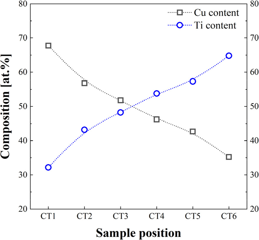
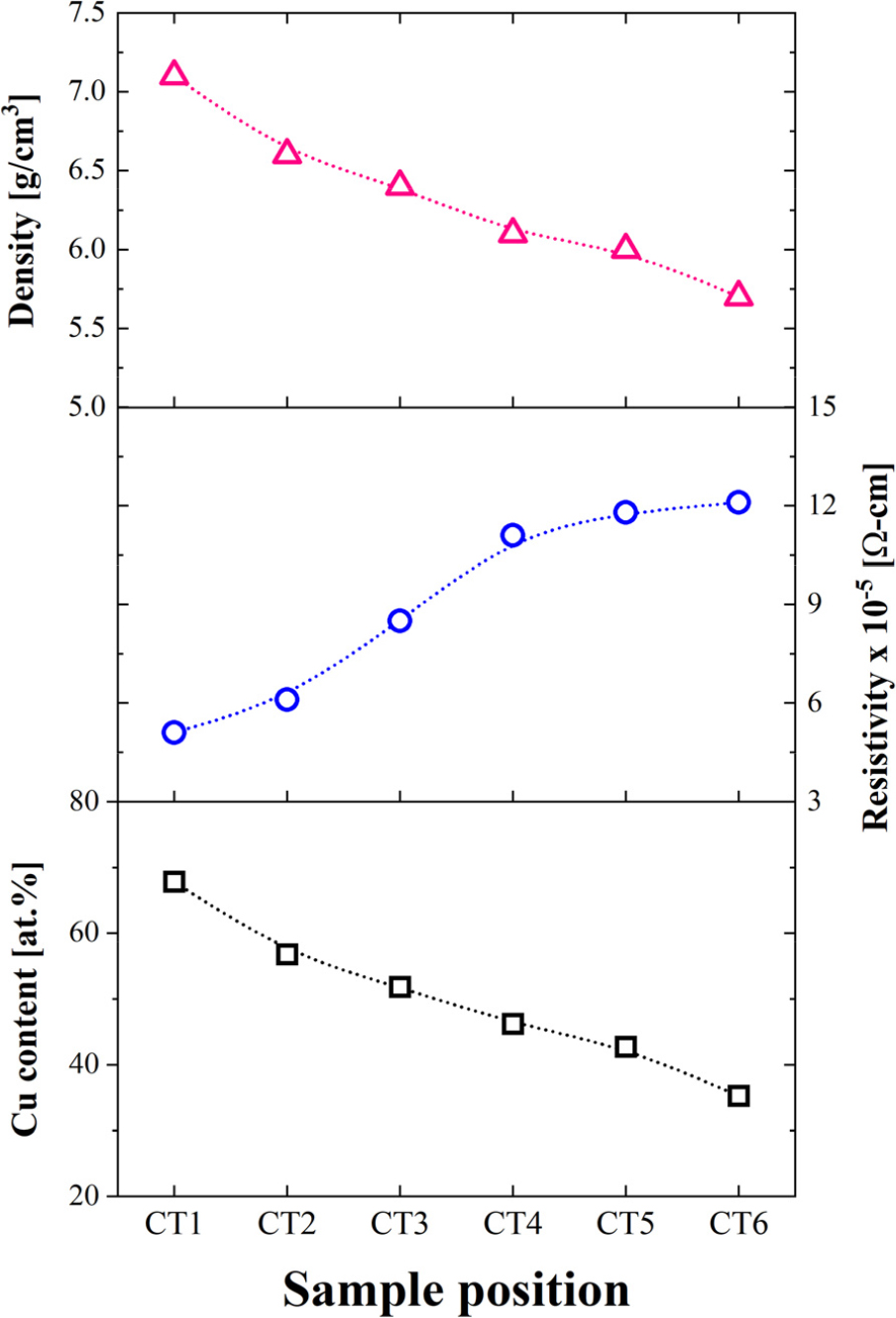
Fig. 2 shows the chemical composition distributions of Cu-Ti films according to the sample position. The Cu and Ti contents of the Cu-Ti films intersect linearly with the increasing sample position. The resistivity and density of the Cu-Ti thin films according to the Cu content is shown in Fig. 3. The resistivity of the Cu-Ti films gradually increases from 5.1 to 12.1 × 10⁻⁵ Ω-cm with the increasing sample position, and the calculated density decreases from 7.1 to 5.7 g/cm3 with the increasing sample number. The Cu-Ti sample library grown by combinatorial sputtering has different compositions, resistivities, and densities according to the sample position, which can be used to derive factors that can improve the performance of SAW devices.
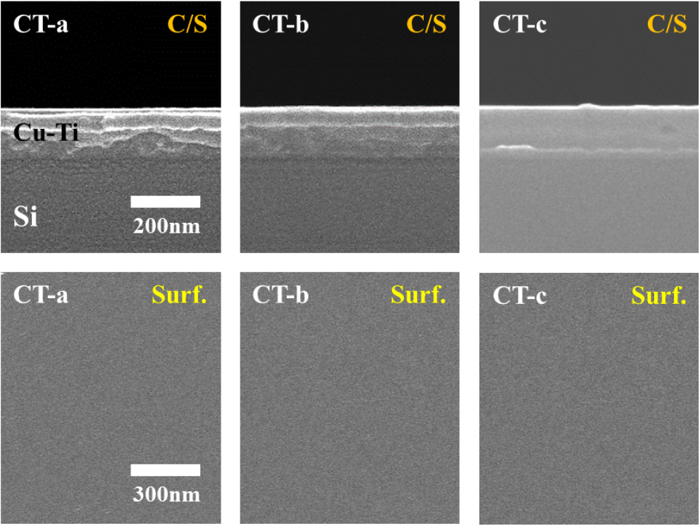
Through combinatorial studies, it was confirmed that the electrical and mechanical properties of Cu-Ti thin films vary with the Cu content at the same film thickness. The SAW-IDT electrodes require low-density materials that can facilitate the generation of acoustic waves by the inverse piezoelectric effect along with outstanding electrical conductivity. Therefore, three kinds of uniform Cu-Ti thin films with different Cu contents were grown on Si substrates, and the composition, resistivity, and density of each sample were closely investigated. Fig. 4 shows three kinds of uniform Cu-Ti films with different Cu contents. The three kinds of Cu-Ti films have the average film thickness of 150 nm, and no structural defects such as voids or cracks were found between the substrate and the film. In addition, all three Cu-Ti samples showed smooth surface morphology, and no defects such as pinholes or cracks were found. A comprehensive study involving the growth of Cu-Ti thin films with compositional gradients was conducted to identify the optimal composition for SAW device applications. The selected compositions, exhibiting uniform properties across the wafer, were successfully applied to the IDT electrodes. This optimization strategy led to a substantial improvement in the overall performance of the SAW devices.
Table 1 shows the chemical composition, resistivity, and density of three kinds of uniform Cu-Ti films. With increasing Cu content in the Cu-Ti films, the resistivity decreased from 10.5 to 5.8 × 10⁻⁵ ohm-cm, and the density increased from 5.5 to 7.3 g/cm3. Importantly, the influence of the SAW-IDT electrodes fabricated using Cu-Ti films with different physical/chemical properties on the acoustic performance of the SAW device were closely investigated.
Table 1.
The chemical composition, resistivity, and density of three kinds of uniform Cu-Ti thin films.
In order to control the solid objects existing in the microfluidics, it is necessary to satisfy the Mie scattering condition because the Helmholtz number () is determined by the relationship between the diameter of the solid object and the resonant frequency. For this reason, the resonant frequency for controlling 5 µm polystyrene (PS) particles in microfluidics was calculated by following Eq. (1).19)
where, is the Helmholtz number, is the resonant frequency and is the speed of acoustic wave in pure water. When the value satisfying the Mie scattering condition is 1.5, the resonant frequency that can control 5 µm PS particles was confirmed to be 143 MHz. To obtain the resonant frequency suitable for 5 µm PS particle separation, the acoustic frequency was calculated by the following Eq. (2).20)
where, is the speed of acoustic wave in the piezoelectric substrate and 𝜆 is the wavelength of SAWs. The wavelength of SAWs is dependent on the structure of IDTs, which can be calculated by the following Eq. (3).20)
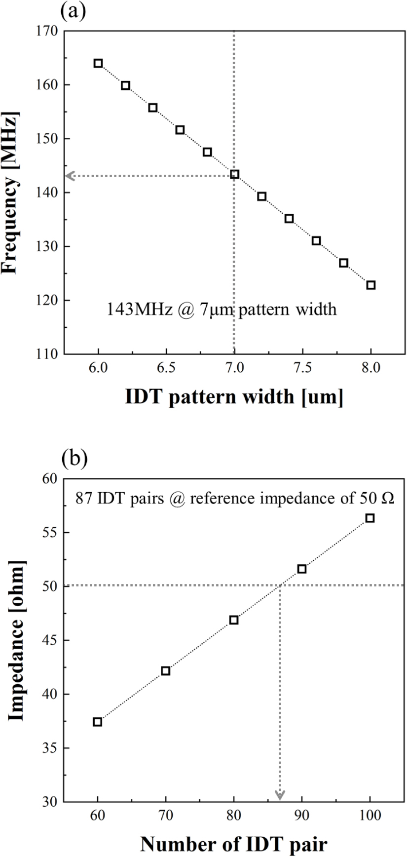
where, 𝜆 is the wavelength of SAWs and is the width of IDTs (assuming the width and the spatial distance of IDTs are the same). Based on the above relationships, the correlation between the IDT pattern width, the number of IDT electrodes, the film thickness, and the total electrode length is clarified through Mathematica, and the influence on the intensity and frequency of the acoustic wave generated from the SAW device is closely investigated. As shown in Fig. 5(a), the resonant frequency corresponding to the IDT pattern width was analyzed using Mathematica, and it was confirmed that the SAW-IDT must be satisfied with the pattern width of 7 µm to obtain the resonant frequency of 143 MHz. Fig. 5(b) shows the relationship between the number of IDT electrode pairs and the total IDT length for impedance matching of the SAW module. In this study, 87 IDT electrode pairs and the total IDT length of 3,000 µm were selected to satisfy the reference impedance of 50 Ω.
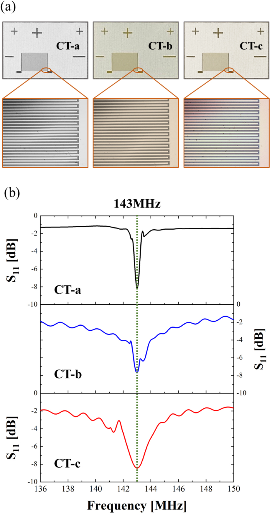
Fig. 6 shows the SAW devices and their resonant frequencies fabricated with Cu-Ti films with Cu contents of 31.2, 48.4, and 71.3 at%, respectively. All three types of SAW devices have the same pattern width of 7 µm, total IDT length of 3,000 µm, film thickness of 150 nm, and 87 electrode pairs. As shown in Fig. 5(b), all three SAW devices exhibited the same resonant frequency of 143 MHz, confirming that they were normally fabricated without any defects in the designed IDT patterns. The SAW device with the Cu content of 31.2 at% showed excellent frequency selectivity with the full width at half maximum (FWHM) value of 0.38 at the main frequency. However, increasing the Cu content in the SAW-IDT electrode can broaden the FWHM values of the resonant frequency, which can drastically deteriorate the acoustic performance of the SAW device. This suggests that the electrical/mechanical properties of the electrode materials, rather than the pattern itself, significantly affect the performance of the SAW device.
The density of the IDT electrode has a direct impact on the generation of SAWs. The higher-density electrode can hinder the propagation of SAWs generated from the piezoelectric substrate, thereby degrading the resonance performance. Therefore, the IDT electrode should ideally possess both low density and high electrical conductivity to achieve optimal performance. In this study, the SAW device fabricated with the CT-a film containing the Cu content of 31.2 at% exhibited the best resonance performance. This is attributed to the synergistic effect of the high electrical conductivity of Cu and the low density of Ti, resulting in optimal electromechanical properties. Pure Ti electrodes, while having low density, suffer from low electrical conductivity, which can degrade the efficiency of the SAW device. In contrast, the CT-a film, through Cu doping, enhances electrical conductivity while maintaining the low density of Ti, significantly improving the performance of the SAW device. In conclusion, this study experimentally confirmed the influence of IDT electrode density on the resonance performance of SAW devices and demonstrated that the performance of SAW devices can be enhanced by optimizing density and electrical conductivity through Cu-Ti compositing.
4. Conclusion
Cu-Ti thin films with the composition gradient were co-deposited using a combinatorial sputtering system to select candidates for IDT electrodes used in SAW devices. The Cu-Ti sample library showed various chemical compositions and electrical resistivities depending on the sample position. To verify the acoustic performance of the SAW device according to the Cu content, three kinds of uniform Cu-Ti thin films were grown on Si substrate. The center frequency was observed at 143 MHz regardless of the Cu content of the SAW-IDT electrode, but the acoustic performance of the SAW device gradually deteriorated as the Cu content of the SAW-IDT electrode increased. As a result, it was verified that the resonance performance of the SAW device can be improved by lowering the density of the electrodes formed on the piezoelectric substrate rather than the electrical characteristics of the IDT electrode.


