

1 Introduction
Transition metal-carbon systems(such as Ni-C, Co-C) have been investigated extensively in literature. To our knowledge, the research interests in this field have been: 1) understanding carbide formation behaviors and crystal structures of these carbides,1-4) 2) disclosing the mechanism of metal mediated crystallization(graphitization) of amorphous carbon,5,6) and 3) exploiting application potentials of these alloy systems.7-9) Both Ni-C and Co-C binary systems compose a simple eutectic phase diagram in the equilibrium state. However, the interactions between Ni, Co and carbon under special conditions appeared to be complex and very interesting. For example, Ni and Co has so far been used as catalyst solvent for the synthesis of diamond under high-pressure, high-temperature conditions. 10) They are also known to mediate the transformation of amorphous carbon to graphite at a temperature as low as 500 °C. The mechanism of such transformation is that carbon atoms dissolve in solid metals and then precipitate as graphite, which is driven by the free energy difference between the amorphous and crystalline state of carbon.5) The non-equilibrium carbides of these metals have also been synthesized via methods such as mechanical alloying, carbon ion implantation into these metals, and thin film technologies.3,4,8 On the other hand, multilayers of Ni/C and Co/C have been found to show high reflectivity for X-rays compared with metallic surfaces and Langmuir-Blodgett films because of the step of the electron density at each metal-carbon interface and the constructive interferences of the reflected beams from all interfaces.7,9) Therefore it is our purpose of this work to expand the knowledge of the interaction between nickel and carbon, and to study the microstructure and properties of Ni-C films as composite materials using a newly developed deposition method. This method combines conventional PVD(ion beam sputtering deposition) and ECR microwave plasma CVD which is widely used to deposit hydrogenated amorphous carbon (a-C:H) films. In this paper, we investigate the microstructure and electrical properties of Ni-C nanocomposite films deposited under various conditions.
2 Experimental Procedure
Ni-C films were prepared in a dual-source deposition system which consists of a Kaufman ion source for ion beam sputtering deposition and an electron cyclotron resonance( ECR) microwave plasma source for CVD. The diagram of the system is shown in Fig. 1. In the present work, the two sources were operated in a co-deposition way; sputtering deposition of nickel with argon ions and chemical deposition of carbon from a discharge of methane and hydrogen gas mixture simultaneously. The substrates used were mainly corning glass slide(25 × 25 mm) for XRD and resistivity measurements, and freshly cleaved surfaces of NaCl (100) for TEM samples deposited at 200 °C or below. For the TEM samples deposited above 200 °C, amorphous SiO supporting films on molybdenum meshes were used directly as substrates.
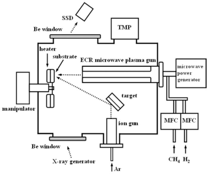
Fig. 1.
Schematic diagram of dual-source deposition system equipped with an in-situ energy dispersive X-ray diffractometer.
Other conditions for the film deposition are listed in Table 1. The films were characterized mainly by X-ray diffraction using Cu Kα radiation, transmission electron microscopy operating at 200 kV. The electrical resistivity of the Ni-C films was determined using the conventional four-point-probe method. And the thickness of the films was evaluated by surface profilometer.
3 Results and Discussion
3.1 Microstructures of Ni-C films
The microstructure of the Ni-C films strongly depends on deposition conditions such as substrate temperature and flow rate of methane(CH4) in the CVD reaction gas mixture. This will be discussed in the following sections.
3.1.1 Ni-C films deposited at low CH4 flow rate
Fig. 2 shows the X-ray diffraction profiles of Ni-C films deposited at a very low CH4 flow rate(less than 0.1 sccm). These results clearly show the formation of hexagonal close-packed (hcp) nickel carbide, Ni3C, at deposition temperatures lower than 400 °C. When increasing the deposition temperature to 400 °C and above, metallic nickel (fcc) phase appeared in the films, which implies that the carbide phase is not stable at temperatures higher than 400 °C. This was also confirmed by annealing of the films after deposition. The results have proved that the carbide phase decomposed into metallic Ni and graphite at about 400 °C.
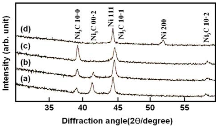
Fig. 2.
X-ray diffraction profiles of Ni-C films deposited at (a) ambient temperature, (b) 300 °C, (c) 400 °C and (d) 500 °C.
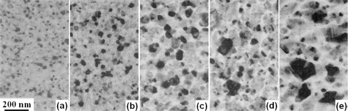
TEM bright field images of the films are shown in Fig. 3. As can be seen from the images, for the films deposited at ambient temperatures(less than 50 °C), the carbide(Ni3C) phase exists in the film as very fine crystallites (about 15 nm in diameter) which disperse uniformly in an amorphous carbon matrix(Fig. 3(a)), while the films deposited at 200 °C and 300 °C reveal granular structures with inter-grain regions as seen clearly in Figs. 3(b) and 3(c). Also, as seen in these images, the size of Ni3C crystallites increases with increasing deposition temperature. It has been demonstrated by the XRD results that a further increase in deposition temperature results in the appearance of metallic nickel (fcc) phase in the films, TEM observation revealed that the microstructure also changes from a granular to a kind of labyrinth structure, as shown in Figs. 3(d) and 3(e).
3.1.2 Ni-C films deposited at higher CH4 flow rates
When deposited at higher CH4 flow rates(> 0.2 sccm), the Ni-C films were found to be amorphous. Fig. 4 shows the TEM bright field images of Ni-C film deposited at a CH4 flow rate of 0.35 sccm, and its electron diffraction patterns(inset).
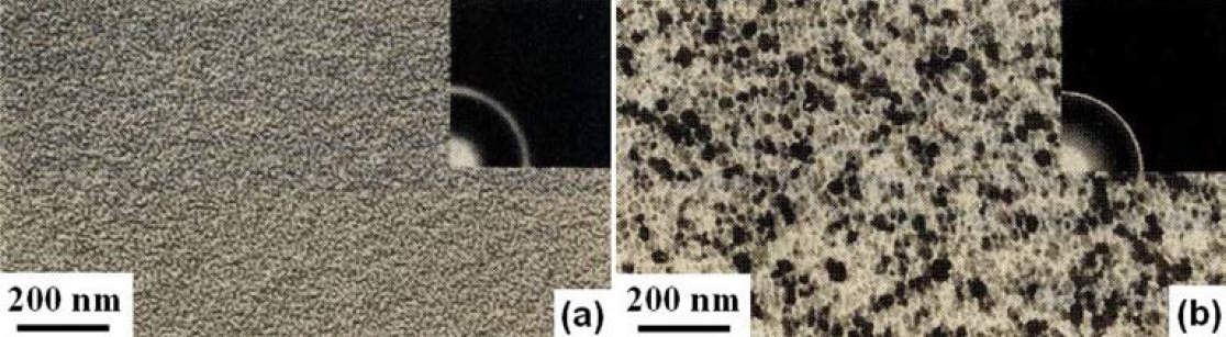
Fig. 4.
TEM bright field images of Ni-C films deposited at (a) ambient temperature and (b) 200 °C(flow rate of CH4 = 0.35 sccm).
The broad diffraction ring for the film deposited at ambient temperature indicated that the film is in an amorphous state. This was also confirmed by X-ray diffraction results. It also can be seen from the image that the microstructure is very fine and uniform throughout the film. Generally, it is extremely difficult to synthesize metal-carbon amorphous alloys by conventional methods such as splash-cooling, because of the high melting temperature of carbon(about 4300 K). For example, a study has shown that even with the addition of another metalloid(silicon, melting point 1683 K), there was no amorphous phase formed in the Ni-C-Si system.11) To our knowledge, this is the first time that the amorphous Ni-C alloy has been synthesized. The mechanism for this is considered to be associated with the high deposition rate of amorphous carbon under present conditions, which prevent Ni and/or Ni3C clusters from growing in the film. This was confirmed by the fact that the deposition rate of Ni-C films at higher CH4 flow rates(~9.08 nm/ min.) is much higher than that at a low CH4 flow rate (1.06 nm/min.), whereas the deposition rate of Ni was fixed through all the experiments. Besides, granular structures were also observed for films deposited at higher deposition temperatures, as shown in Fig. 4(b).
3.2 Electrical properties of Ni-C films
Fig. 5 shows a resistivity change of Ni-C films with flow rate of CH4 and deposition temperature. For films deposited at ambient temperatures, the resistivity increases gradually with the flow rate below 0.2 sccm and thereafter the resistivity goes up abruptly with the flow rate of CH4. This can be explained by the change in microstructure and the increase of carbon content in the films.
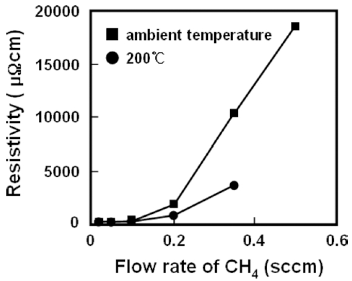
As shown in the previous sections, the microstructures of Ni-C films change from nanocrystallites of Ni3C(at low CH4 flow rates) to amorphous(at higher CH4 flow rates). While, when deposited at 200 °C, all the films reveal granular structures, and the resistivity increases gradually with increasing CH4 flow rate. This increase in resistivity is considered due to the increase of amorphous carbon component in the films. It also should be noted that the resistivity of Ni-C films deposited at 200 °C is lower than that of films deposited at ambient temperatures, which is attributed to the relatively large size of Ni3C crystallites.
The temperature coefficients of resistivity(TCR) for Ni- C films deposited under various conditions are shown in Fig. 6. Ni-C films deposited at ambient temperatures show very low TCR values compared with that of metallic nickel film, and all the films show ohmic characterization even for those in the amorphous state with very high resistivity. Besides, the TCR value decreases only slightly by increasing the flow rate of CH4.
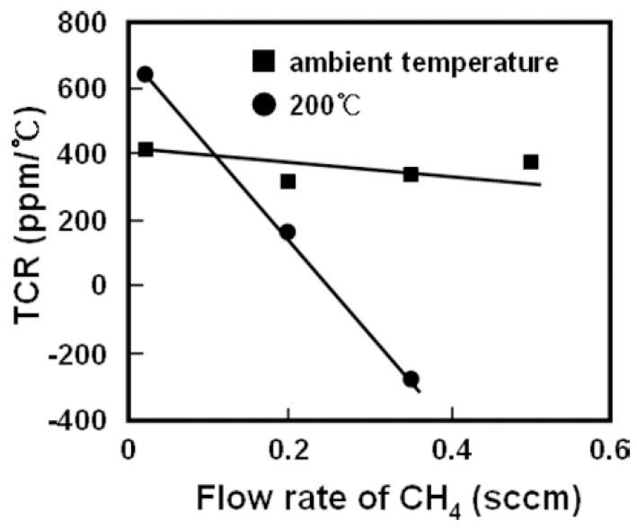
These results have indicated that there is no change in conduction mechanism for these films. It is considered that, even in the amorphous state, metallic nickel and/or nickel carbide clusters form a network in the film, and conduction electrons percolate through the network when an electric field is applied. While, the high resistivity and low TCR value can be explained by the low conduction electron density due to the coexistence of amorphous carbon and the short electron mean free path due to the disordered atomic structure, in which the conduction electrons are severely scattered and trapped. For films deposited at 200 °C, TCR decreases with increasing CH4 flow rate, especially, it changes the sign from positive to negative at a CH4 flow rate of 0.35 sccm. This suggests that different processes are involved concerning the conduction mechanism. As mentioned above, films deposited at 200 °C are featured with granular structures, in which some of the Ni3C grains connect with each other and some of the grains are separated by amorphous carbon. Therefore, the electrical conductivity in this kind of film is considered to be due to the combined contributions of electron percolation through the grains connected with each other and electron tunneling between separated grains.12)
By increasing the CH4 flow rate, amorphous component in the film increases, thus the portion of Ni3C grains separated with each other becomes larger, and the contribution to electrical conductivity due to thermally activated tunneling becomes dominant. This also accounts for the sign change of TCR when deposited at higher flow rate of CH4.
4 Conclusions
A method has been established to synthesize a variety of Ni-C composite films in this work. The microstructures of Ni-C films deposited in these way ranges from amorphous Ni-C alloy to granular structures with Ni3C nanocrystallites. These films are characterized by high resistivity and low TCR value, and the electrical properties can be adjusted over a wide range by controlling the microstructures and compositions of the films.
