


1. Introduction
Increasing demands for high performance transistors for flat panel displays have led to the development of high mobility metal oxide based semiconductors such as In-Ga-Zn-O(IGZO).1-3) Thin-film transistors(TFTs) that use such materials have field effect mobility exceeding 10 cm2/Vs, and are suitable for active-matrix liquid crystal displays(AMLCDs) with ultra-definition (4000 × 2000), large-size(> 70 inch). However, display technology is now oriented towards active-matrix organic light-emitting diode (AMOLED) displays, which need driving transistors with higher field effect mobility.
In this work, an alternative type of high mobility semiconductor, zinc oxynitride(Zn-O-N),4-9) is studied by both theoretical calculations and experimental evaluation of thin films and TFT devices. Hall measurements of reactively sputtered Zn-O-N films indicate that the material is ntype. First principles density functional theory(DFT) calculations are performed to examine the carrier effective mass in pure zinc nitride(Zn3N2), and nitrogen vacancies(VN) are found to be the most dominant shallow donor-like defects. It is shown that doping with metal cations that form a stronger bond with nitrogen leads to the suppression of free carriers, which is confirmed experimentally by doping high mobility Zn-O-N films with gallium(Ga) and aluminum(Al). Thin film transistor devices fabricated using both undoped and Ga-doped Zn-O-N further show such defect reduction, resulting in decreased off-currents and subthreshold swing.
2. Experiment
Thin films of Zn-O-N(50 nm-thick) were deposited onto glass substrates by reactively sputtering a Zn metal target with various ratios of O2/N2 gas flow rates. The sputter process was carried out in a mixture of argon(Ar), oxygen(O2) and nitrogen(N2) plasma. Hall measurements were performed to collect information on the Hall mobility and carrier density. Rutherford backscattering spectroscopy(RBS) analyses were carried out to study the chemical compositions of the films. To fabricate a wafer containing a set of TFT devices, a 200 nm-thick molybdenum( Mo) film was sputtered on a 150 mm × 150 mm square glass substrate and patterned photolithographically to form the gate electrodes. Then, a stack of 350 nmthick silicon nitride(SiNx) and 50 nm-thick silicon oxide (SiOx) films was deposited sequentially by plasma-enhanced chemical vapor deposition(PECVD) to form the gate insulator. After etching the gate contact vias by photolithography, a 50 nm-thick Zn-O-N active layer was deposited by reactive radio-frequency(RF) sputtering.
Different sets of wafers were prepared with active compositions resulting in nitrogen-rich and oxygen-rich ZnON semiconductors. In order to dope the Zn-O-N films, a separate aluminum metal target and a gallium oxide(Ga2O3) ceramic target were used, and were each sputtered along with the zinc metal target. The RF powers applied to the Al and Ga2O3 targets were intentionally modified so that the aluminum and gallium contents in the resulting film could be adjusted. After depositing the active layer, a 100 nm-thick etch stopper layer of SiOx was deposited by PECVD and patterned by photolithography. Finally, a 200 nm-thick aluminum(Al) film was sputter-deposited and patterned by photo lithography to form the source and drain electrodes. Inductively coupled plasma atomic emission spectrometry(ICP-AES) analyses were done to quantify the relative metal cation ratios in the films. The final devices were annealed in air at 250 °C for 1 h, and their electrical parameters were evaluated using a Keithley 4200-SCS parameter analyzer.
Density functional theory(DFT) calculations were performed using the Vienna ab initio simulation package (VASP) code.10,11) The projector-augmented wave(PAW) pseudopotentials12) were used, and the plane-wave basis set with a kinetic energy cutoff of 500 eV was used. The generalized-gradient-approximation(GGA)13) was used with on-site Coulomb energy(U) values of 7.5 and 8 for Zn and Ga d states,14) respectively, for the exchange correlation energy. A 320-atom supercell of Zn3N2 with a cubic anti-bixbyite structure was used for the defect calculations. A 2 × 2 × 2 special-k-point mesh was applied for integrations over the Brillouin zones.
3. Results and Discussion
Hall measurement results are indicated in Fig. 1, where the Hall mobility and carrier density of Zn-O-N films are plotted with respect to the O2/N2 gas flow rate ratios during the reactive sputter process. The transfer characteristics( Id-Vg) of the respective TFT devices are shown in Fig. 2. Note that as the oxygen content increases, the field effect mobility decreases just as observed in the Hall measurements. The drain voltage(Vd) was fixed at 10 V, and the field effect mobility was extracted in the saturation regime for each device.
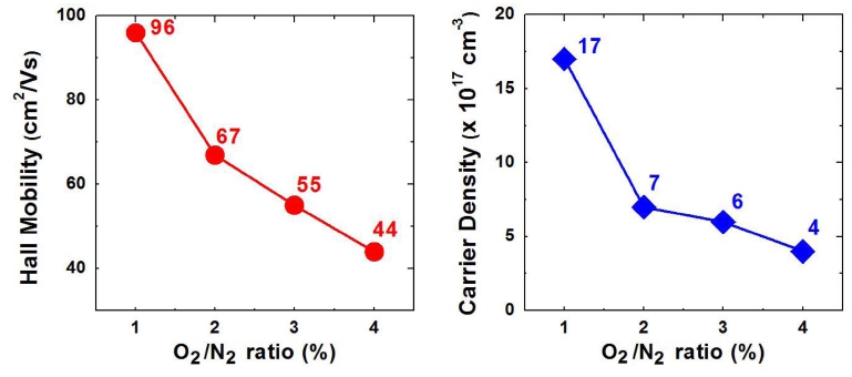
Fig. 1.
Hall mobility and carrier density of Zn-O-N films with respect to the O2/N2 flow rate ratio during the sputter process.
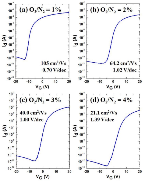
Fig. 2.
Transfer characteristics of TFT devices incorporating Zn-ON active layers, deposited with gas flow rate ratios of (a) O2/N2 = 1 %, (b) O2/N2 = 2 %, (c) O2/N2 = 3 %, and (d) O2/N2 = 4 %. The drain voltage (Vd) is fixed at 10V.
The high mobility film is of interest in this work, and RBS results indicate that the atomic ratio of Zn:O:N is approximately 50:5:45, respectively. It is thus reasonable to assume that the host consists mainly of a nitride matrix, and so to study the types of defects that may form in this material, DFT calculations were done using a crystalline Zn3N2 cubic supercell in the nitrogen-rich regime. The formation energies of the different point defects such as nitrogen vacancy, nitrogen interstitial, zinc vacancy, zinc interstitial, and nitrogen-zinc antisites, are calculated by
where E(X) is the total energy derived from supercell calculations with one defect in the cell. E(Zn3N2) denotes the total energy of pure Zn3N2, and ni denotes the number of atoms of type i(host or impurity) that have been added to (ni > 0) or removed from (ni < 0) the supercell when the defect is introduced. μi is the corresponding chemical potential of the defects, and for example, μN is determined by the energy of a N2 molecule(μN = (1/2) ), and μZn is the total energy per atom in bulk zinc metal.
The calculated formation energies with respect to the Fermi level position within the semiconductor bandgap are plotted in Fig. 3, for the different point defects that may occur in Zn3N2. Nitrogen vacancies(VN) exhibit the lowest formation energies over the entire range, and they tend to exist in a singly charged state as the Fermi level approaches the conduction band minimum. Such a behavior makes them act as shallow electron donors, hence the source of free electrons. This is consistent with the reports that nitrogen vacancies are the major sources of electron carriers in III-V nitride semiconductors.15-17)
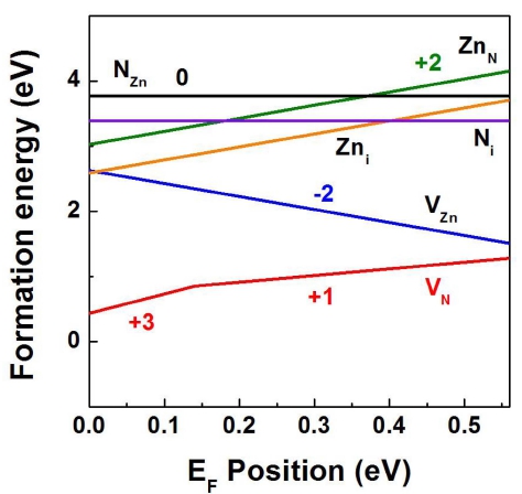
Fig. 3.
Formation energies of point defects in Zn3N2 with respect to the Fermi level position in the semiconductor bandgap.
The formation energies of the different point defects in their neutral states are summarized in Table 1. In order to switch the TFT arrays in a flat panel display, it is necessary to maintain relatively high field effect mobility, while smaller subthreshold swing values are preferred. The incorporation of a metal cation into Zn-O-N semiconductors may be useful in that regard, as a cation substituting Zn that forms a stronger bond with nitrogen is expected to prevent the formation of nitrogen vacancy defects. DFT calculations indicate that gallium(Ga) and aluminum(Al) are good candidates. After replacing a Zn site in the Zn3N2 supercell by either Ga or Al, the neutral VN formation energies were calculated by removing the nitrogen anion adjacent to the dopants, and are indicated in Table 2.
Table 1.
Formation energies of neutral point defects in cubic Zn3N2 based on GGA+U calculations.
| Defect | VN | VZn | Zni | Ni | ZnN | NZn |
|---|---|---|---|---|---|---|
| Ef (eV) Type | +1.97 Donor | +2.69 Acceptor | +5.19 Acceptor | +3.39 Acceptor | +5.39 Donor | +3.78 Donor |
Table 2.
Neutral VN formation energies based on GGA+U calculations when Ga and Al each replace a Zn site in Zn3N2. The VN site under consideration is adjacent to the dopant in each case.
| Dopant | Ga | Al |
|---|---|---|
| Ef (eV) | +2.77 | +2.96 |
Fig. 4 shows the Hall measurement results of Zn-O-N films doped with Ga and Al. As the metal(M) to zinc(Zn) cation ratio M/Zn increases, the Hall mobility decreases and the carrier density decreases by a few orders of magnitude. Fig. 5 shows how the transfer characteristics of a TFT device using undoped Zn-O-N (deposited with O2/N2 flow rate ratio of 1 %) is improved by incorporating Ga (Ga/Zn = 3 %), while keeping a high saturation field effect mobility above 50 cm2/Vs.
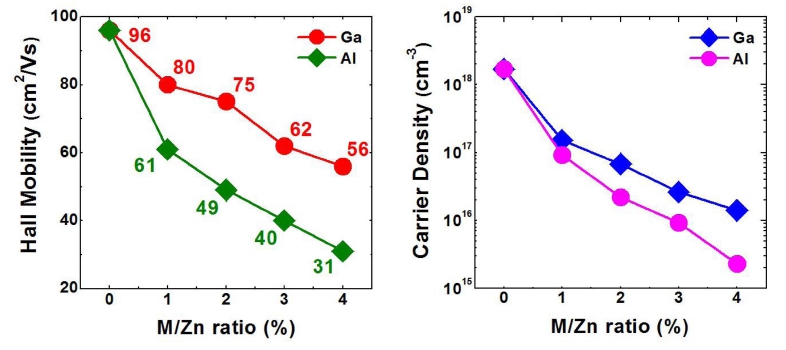
Fig. 4.
Hall mobility and carrier density of Zn-O-N films doped with Ga and Al. The metal (M) to zinc (Zn) cation ratio is denoted by M/Zn.
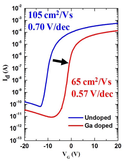
Fig. 5.
Transfer curves of TFT devices using undoped Zn-O-N (flow rate ratio O2/N2 = 1 %) and Ga-doped Zn-O-N active layers (Ga/ Zn = 3 %). The drain voltage (Vd) is fixed at 10 V.
Former reports available in the literature indicate that defects in the semiconductor bulk influence the subthreshold swing of TFT devices, and their reduction results in small swing values.18.19) In the present study, the nitrogen vacancies are believed to also act as the major defects that influence the subthreshold swing, and their suppression by the incorporation of gallium cations is shown to be effective at reducing the subthreshold swing of Zn- O-N devices.
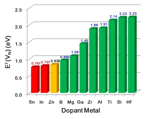
In order to search for metal cations other than gallium or aluminum that form stronger bonds with nitrogen than zinc does, a quick series of DFT calculations was performed with different metal dopants. Here, GGA calculations were carried out in order to observe the relative magnitudes of neutral VN formation energies for a range of metal dopants, and the results are indicated in Fig. 6.
4. Conclusion
In this work, high mobility semiconductors based on Zn-O-N were studied, in terms of thin film electrical properties and TFT performance. DFT calculations revealed that nitrogen vacancies(VN) are energetically most favorable, and act as shallow electron donors. Also, the VN formation energy is found to increase when a Zn cation is substituted by Ga and Al, which form strong bonds with nitrogen. The incorporation of Ga or Al in Zn-O-N results in the suppression of excess free carriers, occurs by the reduction of VN defect density. It is suggested that the reduction of shallow VN defects also helps to reduce the subthreshold swing in the transfer curves of cation-doped Zn-O-N devices. In terms of nitrogen vacancy formation energies, a preliminary analysis by DFT calculations suggests a variety of metal dopants that may act as carrier suppressors in the zinc oxynitride system.