

1. Introduction
Low-dimensional (2D) materials such as graphene,1) boron nitride2) have been attracting special attention of scientists due to their unusual mechanical and electronic properties. Following those findings, other groups of 2D materials such as chalcogenides,3,4) dichalcogenides,5,6) borophene7) have been discovered and studied. Their distinct electronic and thermal properties are also revealed in turning and becoming important bases for applications in micro-electromechanical systems, opto-electrical devices, thermoelectrics, sensors.2,5,6,8,9)
The group of chalcogenide materials containing lead (Pb) exists in numerous distinct structures, comprising α, β, γ, 1T and 1H,10-12) that have been proven to have high potential for applications in electronic and optical devices. Previous studies have primarily focused on the α, β, γ or 1T structures, while the 1H-PbX2 structure has not been widely investigated. Jin et al. have indicated that the multifunctional material structure PbS2 has a negative Poisson’s ratio and electronic properties that can be controlled by strain.13) In the study by Quain, the heterostructure of Pb coated on WS2 material has the potential to enhance the performance of the devices, facilitating the development of optoelectronic applications.10) The electronic and thermal properties of several chalcogenide materials containing Pb have also been explored.14) Meanwhile, 1H-MX2 structures with M of transition metal, that have many practical applications, such as high-efficiency electroreduction,15) conversion and generation of new energy sources, and other applications.16) Therefore, in this paper, we investigate the mechanical and electronic properties of 1H-PbS2 and 1H-PbSe2 in order to determine their potential applications in the near future.
2. Simulation
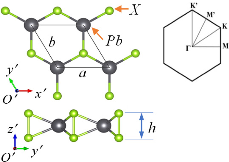
In this study, all calculations were performed by the density functional theory (DFT)17,18) with Perdew-Burke-Ernzeholf exchange correlation potential energy (PBE) using the generalized gradient approximation (GGA)19) implemented in Quantum Espresso package.20) The kinetic energy cutoff was chosen as 60 Ry for the wave function and 700 Ry for the charge density. The kpoint grid in the Birilluoin region was selected as 15 × 15 × 1 according to the Monkhorst-Pack method.21)Fig. 1 depicts the atomic structures of 1H-PbS2 and 1H-PbSe2. Periodic boundary conditions were applied on all three x, y, z directions of the model. The vacuum region in the z direction was set to 30Å to avoid interaction between atomic layers. The equilibrium structure was obtained by the Broyden-Fletcher-Goldfarb-Shanno (BFGS) minimum energy method with the stress components less than 5.10-2 GPa and the force conditions less than 5.10-6 Ry/a.u at the temperature 0K.22) The elastic constants are calculated using the Thermo-Pw algorithm.23) The structure is investigated under the strain in the x, y and biaxial directions with the step of 1 % until the material structure is fracture. The strain is defined by ε = (a – a0) / a0, where a and a0 are lattice constants of 1H-PbX2 (X: S, Se) after and before applying the strain.
Eqs. (1) and (2) are given to determine the elastic moduli Exx, Eyy and Poisson’s ratios υxy, υyx via the elastic constants Cij:6,24)
3. Result and Discussion
Based on the density functional theory, the material parameters such as lattice constant a, b, elastic constant Cij determined are listed in Table 1. The obtained results show that the lattice constant increases as the element X changing from S to Se as a = b = 4.73 (Å) and a = b = 4.88 (Å), respectively. The gradual increase of the lattice constant is due to the increasing radius of chalcogenide elements.
Table 1.
Lattice constant a and b (Å), thickness h (Å), elastic constant Cij (N/m), elastic modulus E (N/m) and Poisson’s ratio υ of 1H-PbS2, 1H-PbSe2 materials.
| Material | a = b | h | C11 | C22 | C12 | C66 | Exx = Eyy | υxy = υyx |
| 1H-PbS2 | 4.73 | 2.15 | 28.70 | 28.70 | 26.87 | 0.86 | 3.54 | 0.94 |
| 1H-PbSe2 | 4.88 | 2.42 | 25.90 | 25.90 | 24.63 | 0.64 | 2.48 | 0.95 |
Based on Born’s criterion25) with C11 > |C12| > 0 and C66 > 0, two material structures confimed to be stable. The elastic modulus of monolayer structures 1H-PbS2 and 1H-PbSe2 are Exx = Eyy = 3.54 N/m and Exx = Eyy = 2.48 N/m, respectively, which are significantly smaller than the elastic modulus of other 2D structures such as GaInTe3 (113 N/m)26) or Janus WSSe (137.7 N/m)27) or 1H-WS2 (220 N/m).6) This result shows that the monolayer structures 1H-PbS2 and 1H-PbSe2 can be used in applications with large mechanical strain.
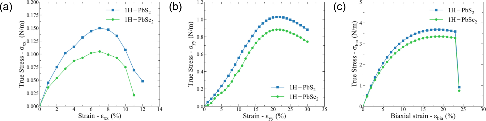
Fig. 2 shows the stress-strain relationship in the x, y and biaxial directions. Due to the monolayer structure, the stress is calculated as the product of the unit cell stress (N/m2) and the unit cell thickness (30 Å).28) Generally, the stress-strain relationship of the two structures is similar in all three directions x, y and biaxial. The ideal strain of 1H-PbS2 is higher than that of 1H-PbSe2 in all three directions. The maximum stress in the x direction of 1H-PbS2 [Fig. 2(a)] is 0.15 N/m at εxx = 7 %, about 0.04 N/m higher than 1H-PbSe2. Under the strain εyy, two materials are failed at the relatively large strain (εyy = 22 %) with the critical stress of 1.03 N/m for 1H-PbS2 and 0.88 N/m for 1H-PbSe2. Finally, the critical stresses in the biaxial direction of 1H-PbS2 and 1H-PbSe2 are 3.48 N/m and 3.68 N/m, respectively at the strain of 19 %. The strength of 1H-PbS2 is higher than that of 1H-PbSe2 because the electronegativity of S (χ = 2.58) is greater than that of Se (χ = 2.55), which makes the bond of Pb-S more difficult to break than that of Pb-Se.
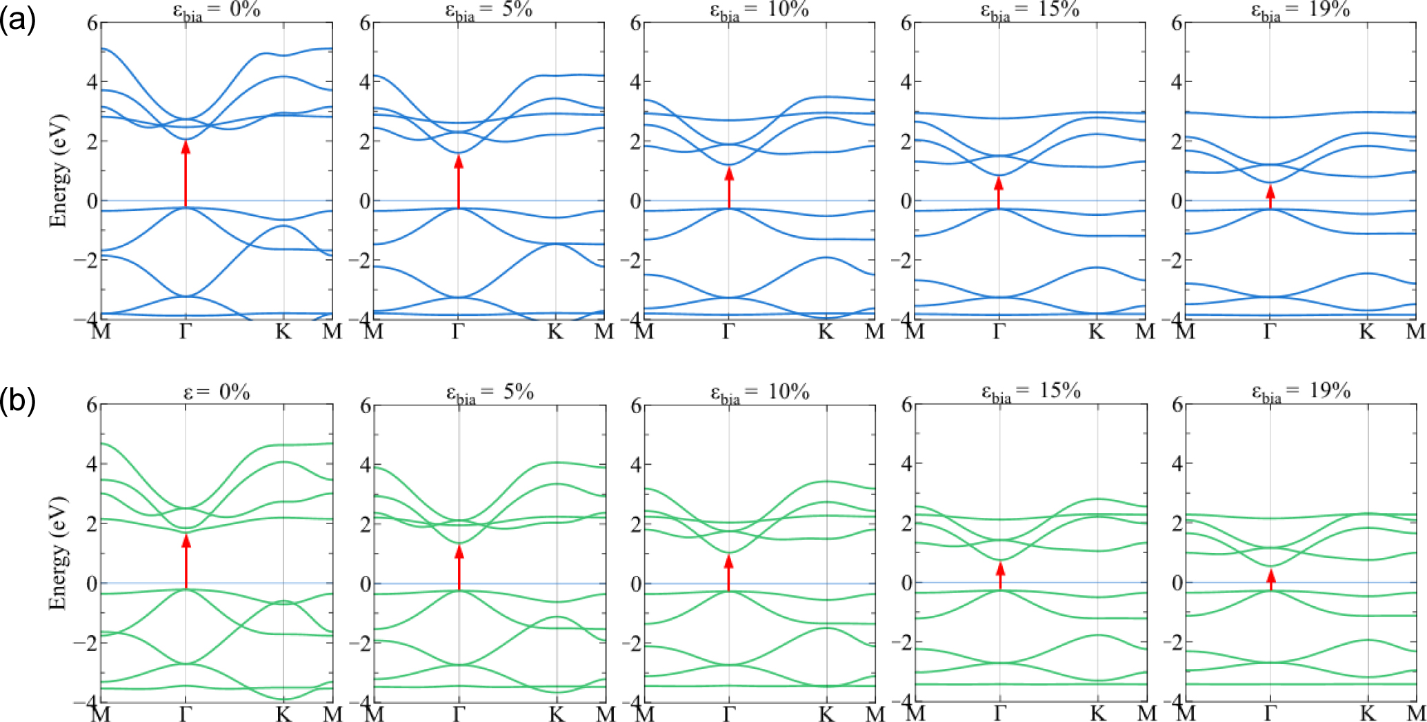
To understand more the strain effect on the electronic properties, the band structure of 1H-PbS2 and 1H-PbSe2 is investigated at several strains. In Figs. 3 and 4, 1H-PbS2 and 1H-PbSe2 possess the band gap at the equilibrium (ε = 0 %) of 2.30 eV and 1.90 eV, respectively. The results show that two materials are both the direct semiconductors with the conduction-band minimum and the valence-band maximum both at the point. Fig. 3 shows the strain effect in the x and y directions on the band gap of 1H-PbS2. Under the strain εxx, the band gap insignificant change at the fracture strain (εxx = 7 %). The material remains the direct semiconductor. Under the strain εyy, the band gap tends to decrease. The valence-band maximum remains at the Γ point, however the conduction-band minimum moves from the point to K’. The material changes from the direct semiconductor to the indirect semiconductor in this case.
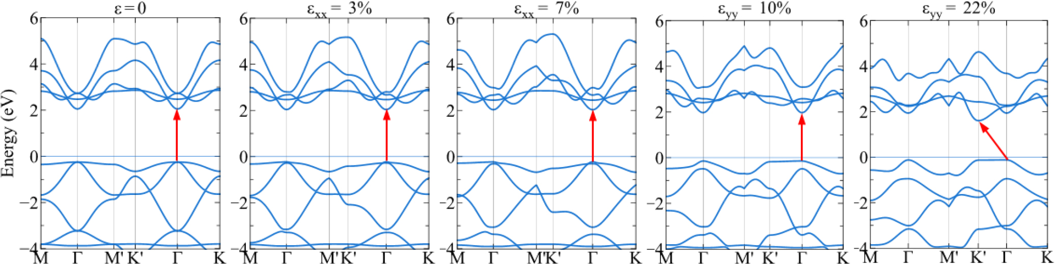
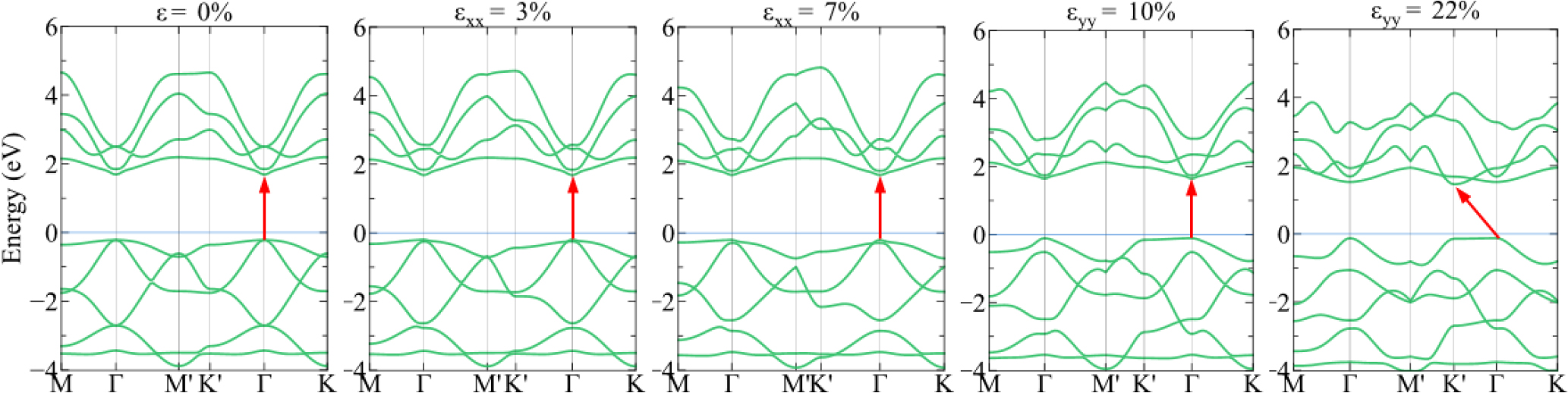
Fig. 4 shows the energy band structure of 1H-PbSe2 at several strains in the x and y directions. Similar to 1H-PbS2, the obtained results show that 1H-PbSe2 remains the direct semiconductor, and the band gap does not change significantly under the tensile strain εxx. The material also changes from the direct semiconductor to the indirect semiconductor under the strain εyy = 22 %.
In Fig. 5, under the strain εbia, 1H-PbS2 and 1H-PbSe2 both exhibit the direct semiconductor, however their band gap decreases significantly with increasing the strain. At the equilibrium (0 %), 1H-PbS2 and 1H-PbSe2 possess the band gap of 2.3 eV and 1.9 eV respectively, but at the fracture strain (19 %), the band gap of 1H-PbS2 is decreased about 60 % and 1H-PbSe2 decreased about 50 %.
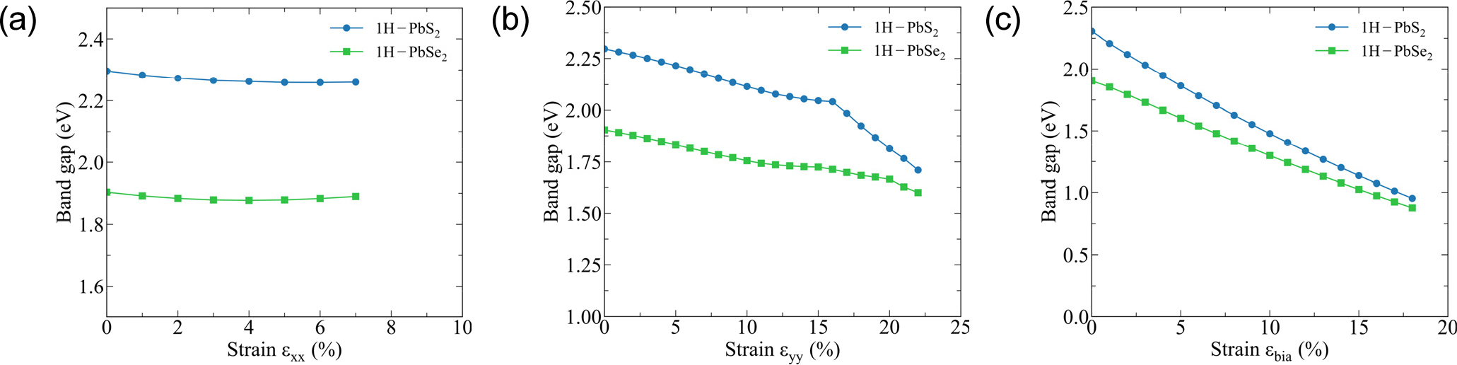
The relationship between the band gap and strain is shown in Fig. 6. Overall, results express that the band gap in almost constant under the stain εxx, Fig. 6(a). Under the strain εyy, the band gap of 1H-PbS2 declines slightly. While, the band gap of 1H-PbSe2 decreases more significant than of 1H-PbS2. The least band gap of both models is 1.71 eV (decreasing by 25.5 %), 1.6 eV (decreasing by 16 %) respectively relating εyy = 22 %, Fig. 6(b). Additionally, under biaxial strain, the band gap of 1H-PbS2 and 1H-PbSe2 plummetes swiftly to destructive strain (εbia = 19 %), as illustration above. To sum up, the band gap is function of mechanical deformation. Each strains and kind of deformation will have sole band gap. While, the band gap involving strain εxx has moderately change, the band gap of strain εyy and εbia decline dramatically to fracture strain in both structures 1H-PbS2 and 1H-PbSe2. Moreover, the obtained results show that the 1H-PbS2 and 1H-PbSe2 account the particularly band gap, direct and indirect properties that can be changed through mechanical deformation under the strains εxx, εyy and εbia. This change is similar to the Janus TMDs MoSSe, WSTe, WSeTe.27) The obtained results once again confirm that the band gap of the material can be controlled by mechanical strain.
4. Conclusions
Based on the density function theory, the mechanical properties and the strain effect on the electronic properties of 2D material 1H-PbX2 (X: S, Se) are investigated. The obtained results show that the materials possess the greatest ideal strength in the biaxial strain with 1H-PbS2 of 3.48 N/m and 1H-PbSe2 of 3.68 N/m. At the equilibrium (0 %), 1H-PbS2 and 1H-PbSe2 are both the direct semiconductors with their band gaps of 2.30 eV and 1.90 eV, respectively. Under the strain εxx, the band gap of two materials is almost unchanged, however they alter significantly under the strains εyy and εbia. At the fracture strain in the biaxial direction (19 %), the band gap of 1H-PbS2 decreased about 60 % and that of 1H-PbSe2 decreased about 50 %. Interestingly, under the strain εyy, 1H-PbS2 and 1H-PbSe2 convert from the direct to the indirect semiconductor. The results obtained above are an important basis for using mechanical strain to control the band gap as well as to convert materials from the direct to the indirect semiconductor.
