


1. Introduction
Grain size and residual stress in films are strongly related to microstructures including texture and columnar structures in the films, especially for the metallic films of Mo, W and Al, having cubic symmetry which can be obtained by dc magnetron sputtering, by which a substrate usually faces a target.1-3) Thornton studied film textures in relation to sputtering gas pressure and substrate temperature, and proposed a structure model which involves morphological characteristics in such sputtered films.4) After his studies, many researchers have effectively used this model to explain film microstructures in the sputtered metallic films. It should be noted, however, that he did not account for the relationship between preferred crystallographic orientation and microstructure in such films, and this sometimes led to a misunderstanding of the structure model. Oya et al. and Flink et al. investigated microstructures in Ti films prepared by dc sputtering in relation to the crystallographic orientation of columnar structures, and demonstrated experimentally that a oneto- one correspondence does not always exist between the preferred orientation and columnar structure in the film, especially for metallic films such as Ti films which have different crystallographic anisotropy from cubic symmetry.5,6) These experimental results suggested that the sputtering gas pressures affect the microstructures in the Ti films, and thus the electric resistivity and related thermal coefficient in Ti films vary strongly with sputtering gas pressures.
The aim of this study is to confirm such speculations experimentally. The effect of masking on film texture was also studied by changing the thickness of a masking plate (or a mask) which is used for the deposition of a designed shape. We discuss the correlation between electric resistivity and film texture in such Ti films on the basis of results obtained.
2. Experimental Procedure
Ti films were prepared by a dc sputtering apparatus of two-facing-targets type at room temperature. The apparatus has characteristics that a magnetic field of about 0.02 T is applied perpendicularly to the target surface by the aid of permanent magnets placed behind both targets, and thus plasma is confined to a region between the two targets, and thereby the bombardment of ions onto deposited films is avoided, resulting in slight damage and low substrate temperature.7,8) Two Ti disks (purity: 99.99 %), 100 mm in diameter and 10 mm thick, were used as target materials and placed at a distance of 150 mm from each other, and several substrates were placed perpendicularly to and far away from the targets. Variable experimental parameters were Ar gas pressure of 0.1 to 1.0 Pa, discharge voltage of 230 to 340 V, discharge current of 1.0 A, sputtering time of 1 to 7 h and deposition rate of 8 to 13 nm/min depending on applied voltage at ambient temperature. The films of 0.5 and 3.0 μm thick were deposited at ambient temperature onto slide glass plates by using masks of different thicknesses of 0.4 and 1.0 mm. The degree of preferred orientation was evaluated by X-ray diffractometry(θ-2θ) using CuKα. Microstructures including film texture and columnar structure were observed through a high resolution scanning electron microscope. The in-plane electric resistivity of the film was measured by a conventional four-probe method with a constant current of 10 mA at room temperature. In addition, the thermal coefficient of resistivity was measured in a temperature range from 260 to 373 K by a simple heating-cooling apparatus equipped with a Peltier device.
3. Results
3.1 Film texture and sputtering gas pressure:
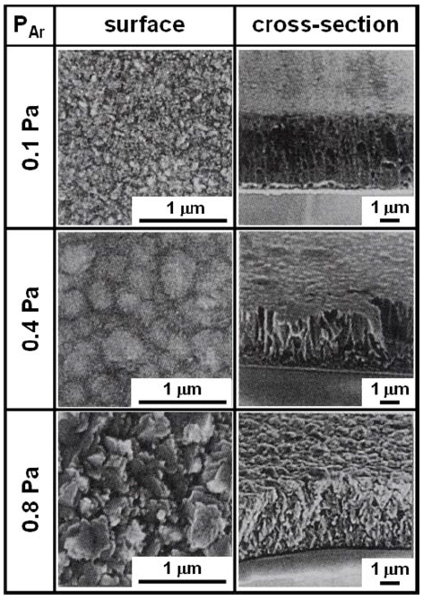
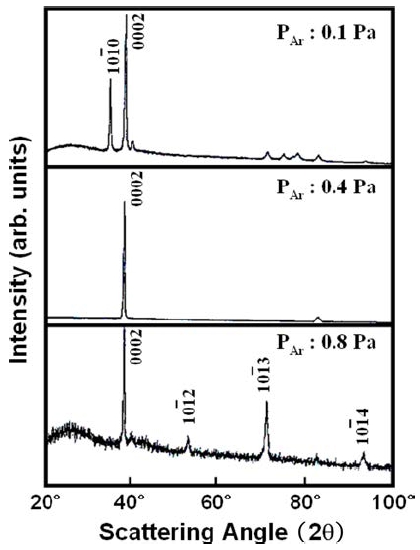
Fig. 1 represents typical examples of cross-sectional microstructures and surface morphology in as-deposited Ti films which were deposited under various sputtering gas pressures. The morphological features including columnar structures and surface roughness can be well explained on the basis of Thornton's zone mode4): column's diameter increases with increasing gas pressures. The film deposited at 0.8 Pa exhibits cross-sectional microstructures composed of grains stacked in the direction normal to the substrate surface, resulting in less massive columnar structure. Thus surface roughness seems to be enhanced on account of the size of individual grains. Detailed observations of such films revealed that fine gaps were seen between neighboring grains. Fig. 2 represents the X-ray diffraction pattern of as-deposited Ti films of 3.0 μm thick, deposited with a 1.0 mm thick mask. The characteristics of X-ray profiles were nearly the same for the films of 0.5 μm thick. The deposited films were found to be α-Ti (hcp) phase. It is shown from these X-ray results that the preferred orientation of the films varies strongly with the sputtering gas pressures irrespective of film thickness: the film deposited at 0.4 Pa shows the highest preferred (0001) orientation among three films shown in Fig. 1, and the film deposited at 0.8 Pa appears less preferred than the others. The relationship between the film texture and the preferred orientation will be discussed later.
3.2 Resistivity and sputtering gas pressure:
Fig. 3 represents the variations of electric resistivity with sputtering gas pressures for the Ti films of different thicknesses, 0.5 and 3.0 μm, and these films were deposited with a 1 mm thick mask under various gas pressures. A minimum of resistivity is seen around 0.4 Pa for both films, and the apparent tendency is almost the same for the two films with a small difference in resistivity because of the different film thickness: the thicker, the lower resistivity. The films deposited at high gas pressures show higher resistivities.
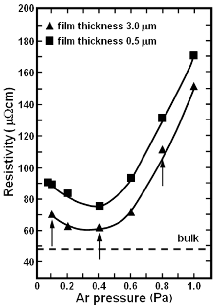
Fig. 3
Resistivity as a function of sputtering gas pressure for Ti films deposited with different thicknesses.
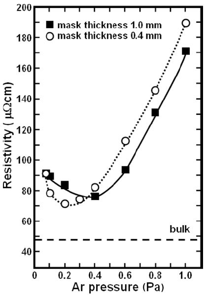
The thickness of mask is thought to have an effect on film deposition as shown in Fig. 4. The deposited films of 3.0 μm thick, thus, were also examined in terms of resistivity at the two mask thicknesses, 0.4 and 1.0 mm. When the films were deposited with a 0.4 mm thick mask, they showed a minimum at a slightly lower gas pressure than that with a 1.0 mm thick mask. It can be seen that masking is strongly related to film deposition. It is thought that the effect of masking is strongly related with the changes in microstructure of the film, thus resulting in different resistivity. The results show that there exists a strong correlation between resistivity and microstructure in terms of sputtering gas pressures, being irrespective of film thickness.
3.3 Thermal coefficient of resistivity and sputtering gas pressure:
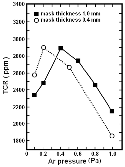
The resistivity of material is also characterized by the thermal coefficient of resistivity(TCR). Thus TCR was measured for the films deposited under different gas pressures. As a result, the TCR was found to be constant in a measuring temperature range. Fig. 5 shows the results of the TCR as a function of sputtering gas pressure for the films deposited with different mask thicknesses. The shadowing effect due to masking is expected to be different for both films. The films deposited with a 0.4 thin mask show a maximum of TCR at slightly lower gas pressures than that with a 1.0 mm thick mask. The maximum of TCR is also seen around 0.4 Pa, which is the same as the relationship between resistivity and gas pressure, as shown in Fig. 4. The relationship between resistivity and TCR, which can be seen from a comparison between Figs. 4 and 5, is generally observed in ordinary materials. Thus, it can be said that the films with higher resistivities always exhibit lower TCRs.
3.4 Sputtering gas pressure and the lattice spacing
When the films are deposited without mask under various gas pressures, they exhibit different lattice spacings, as shown in Fig. 6, where the variations of the lattice spacing are plotted as a function of sputtering gas pressure.
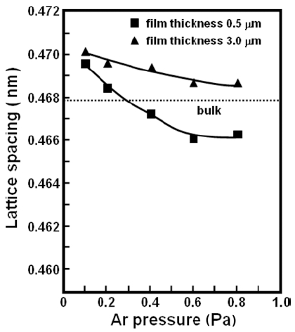
Fig. 6
Variations of the lattice spacing of as-deposited Ti films formed under various sputtering gas pressures.
In this study the lattice spacing was evaluated by only the angular position due to the 0001 peak. The lattice spacing also decreases with increasing sputtering gas pressures for both films of 0.5 μm and 3.0 μm thick. The lattice spacings are slightly larger than those of the bulk crystal at lower gas pressures, indicating that the asdeposited Ti films are in compressive state when deposited at lower gas pressures. Such a phenomenon was already reported for Fe films which were deposited in the same dc sputtering apparatus and it demonstrated that the films are constrained to be strained owing to the atomic shot peening effect of sputtered particles.8,9) It is also reported that Ti films deposited by rf sputtering with high deposition rates are in compressive state.10) Therefore, the observed tendency of the lattice spacing can be ascribed to the existence of film stress caused during deposition. Fig. 6 indicates that thinner films are much easier to be strained by sputtering gas pressures than thicker ones.
4. Discussion
The relationship between microstructure and resistivity is discussed on the basis of experimental results obtained in this study. Taking into consideration the X-ray results which reflect the characteristics of textures in as-deposited films, information concerning preferred orientation of the films can be obtained. Less preferred orientation is expected for the films deposited at 0.4 Pa, they are composed of columns with small diameters, resulting in a large number of column boundaries in the unit area of the film. The films deposited at 0.8 Pa are composed of randomly oriented grains, resulting in a large number of grain boundaries. On the contrary, the films deposited around 0.4 Pa show the most preferred (0001) orientation among the films examined. They are thought to have more regular boundaries than randomly oriented films. These experimental results allow a quantitative explanation about the relationship between resistivity and microstructure in Ti films as follows: In general, the resistivity of film is strongly influenced by grain or column boundaries in the film as well as crystal defects including fine gaps between neighboring columns or grains introduced during deposition process, and they play the role of scattering site of electrons. Thus, the films having a well preferred orientation in the film are expected to exhibit relatively low resistivities, and less preferred films can exhibit relatively large resistivity. This speculation is consistent with the present experimental results obtained in the Ti films. However, the reason why the Ti film exhibits the most preferred (0001) orientation at a sputtering gas pressure of 0.4 Pa is not clear yet. This is probably due to the geometrical arrangement of target and substrate in the sputtering apparatus used. A similar tendency is expected to occur especially for metallic films which have crystallographic anisotropy such as hexagonal symmetry.
When the films are heavily strained by crystal defects, they can show slightly higher resistivity than that of slightly strained ones. The results shown in Fig. 6 mean that the film of 3.0 μm thick is less strained than that of the film of 0.5 μm thick, and thus the former can have a slightly lower resistivity than the latter. In fact, this is confirmed with the results shown in Fig. 3, where the former shows a slightly lower resistivity than the latter. Previous study demonstrated that the films showing the preferred (0001) orientation are in a small stress state on account of stress relaxation occurring on the (0001) basal planes.5,6) This is also consistent with the fact that the preferentially (0001) oriented films deposited at 0.4 Pa exhibit relatively low resistivity.
As expected theoretically, the mean free path of sputtered particles decreases with increasing sputtering gas pressure under the present sputtering conditions. A simple estimation of such mean free paths suggests that the sputtered particles including Ti and Ar atoms and Ar ions can have shorter mean free paths than 1 cm under sputtering gas pressures of 0.3 to 0.8 Pa. At lower gas pressures the mean free path increases apparently with decreasing sputtering gas pressure. This suggests that the shadowing effect due to sputtered particles on film texture can be enhanced at higher sputtering gas pressures, and that the shadowing effect can be also affected by the thickness of mask. The occurrence of fine gaps, which were observed between neighboring grains and remarkable for the films deposited at 0.8 Pa, can be ascribed to the shadowing effect at higher sputtering gas pressures. The results in Fig. 4 also indicate that a thin mask can allow sputtered particles having slightly larger mean free paths to deposit onto substrates more easily than a thick mask. Therefore, the use of thinner masks may be equivalent to the deposition at lower gas pressures.
5. Conclusions
The in-plane resistivity of as-deposited Ti films was measured for various preparation conditions. It is shown that the resistivity is strongly dependent on sputtering gas pressures under which the films are deposited, and that the resistivity is very sensitive to the microstructures including texture and columnar structures. These features are thought to be remarkably actualized in the films which have noncubic symmetry. When the microstructure of the film is first examined in terms of sputtering gas pressures, the resistivity measurement of such a film will play a monitoring role which can provide information concerning film texture or columnar structure without destruction of the film. In this study, it can be concluded that Ti films which have relatively low resistivities are composed of well preferentially oriented columns.