

1. Introduction
Metal/polymer composite films have been widely used in a variety of microelectronics.1-3) With the recent growth in mobile phones and wearable electronics, there is growing demand for metal/polymer composite films with high functionality, low defect rate, and extended product lifetime. One of the key factors determining the defect rate and product lifetime is the adhesion between the plated metal film and the polymer substrate. To improve the adhesion, various polymer surface modification methods have been studied, including chemical etching,4,5) plasma etching,6-8) laser etching,9) and ion beam etching.10,11) Many studies have reported that increased surface roughness contributes to an increase in interfacial adhesion.12,13)
As a conducting metallic film in metal/polymer composite films, copper with a high electrical conductivity is most widely used. Among the various types of polymers, polyethylene terephthalate (PET) has not only beneficial thermal and mechanical properties, but also excellent transparency. For these reasons, PET is extensively used in a wide variety of electronic devices and display panels.14-16)
Cu/PET flexible composite films have been fabricated using electroless plating in our research group. Because electroless plating is a wet plating method, the wettability of the plating solution on the PET substrate is very significant for improving the adhesion between the Cu and PET. The poor adhesion between the Cu and PET was overcome by performing surface modification of the PET using oxygen plasma, which can not only enhance the wettability of the plating solution, but also increase the roughness of the polymer surface and consequently increase mechanical interlocking.17,18) The surface modification of the PET using oxygen plasma produced an anisotropic nanostructure morphology on the PET surface. To maximize the Cu/PET interfacial adhesion strength, the shape and size of the anisotropic nanostructures of the PET surface was controlled by significantly varying the oxygen plasma etching time. The effect of changes in size and shape of super-hydrophilic anisotropic nanostructures on the Cu/PET interfacial adhesion was analyzed. The peel strength of the Cu/PET interface increased with increasing plasma treatment time, and then decreased after reaching the maximal value.19) Such a change in peel strength depends on the nanostructure of the Cu/PET interface. However, no in-depth study on the reason for the change in peel strength has been made.
In this work, the failure mechanism of the Cu/PET flexible composite films depending on the shape and size of the Cu/PET interface nanostructure was studied from the observation of the cross-sections and surfaces of the fractured specimens. Such a change in peel strength of the Cu/PET interface was explained on the basis of the failure mechanism.
2. Experimental Details
PET was purchased from Toray (Tokyo, Japan). PET films with dimensions of 100 mm (length), 40 mm (width), and 100 mm (thickness) were cleaned ultrasonically in ethanol and deionized water, and then dried with N2 gas. The cleaned films were plasma-treated for different times (7, 15, 30, 60, 90, and 120 min) in a vacuum chamber. The oxygen gas pressure, oxygen flow rate, and bias voltage for the plasma treatment were 10 mTorr, 20 sccm, and -400 V, respectively.
Fig. 1 shows the experiment flow chart showing the procedure to fabricate the Cu/PET flexible composite film used for 90° T-peel test. The plasma-treated surfaces of the PET films were coated with copper layers using electroless plating. After electroless plating for 10 min, the thickness of the Cu films was 200 nm.
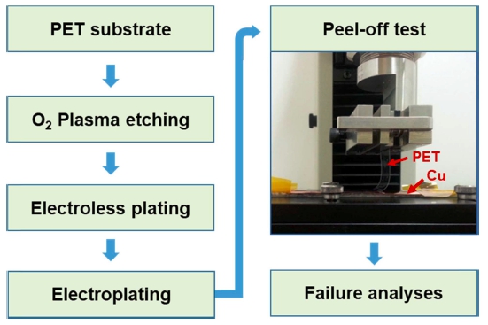
Fig. 1
Experiment flow chart showing the procedure to fabricate the Cu/PET flexible composite film used for 90o T-peel test. Because the Cu layer fabricated by electroless plating is not thick enough to peel off, electroplating was performed additionally to increase the thickness of the Cu layer on PET.
The surface roughness of the samples was determined using an optical surface profiler (M-surf, Nanofocus AG). Peel-off-tests were carried out to measure the adhesion strength between the Cu coating layer and the PET substrate film. A universal testing machine (MTS Insight 1) with an attached 90° T-peel test rail was used. Because the Cu layer initially fabricated by electroless plating was not thick (200 nm) enough to peel off, additional electroplating was performed to increase the thickness of the Cu layer on the PET. The final thickness of the Cu layer after the additional electroplating was 100 mm. The dimensions of the PET films used for the peel-off-tests were 100 mm (length) × 20 mm (width) × 100 mm (thickness). When a thick Cu layer is peeled off during a peel-off-test, the peel strength cannot be exactly measured because of the energy loss due to bending of the thick Cu layer. In this study, therefore, the PET layer was peeled off as shown in Fig. 1. The details of the experiments were described earlier.19)
A field emission scanning electron microscope (FESEM, S-4800, HITACHI) was used to observe the morphologies of the anisotropic nanostructures on the plasma-treated PET surfaces, and the cross-sections and surfaces of the fractured specimens after the T-peel tests. From observation of the morphologies of the anisotropic nanostructures, the Cu/PET interface area and nanostructure width were analyzed. From observation of the crosssections and surfaces of the fractured specimens after the T-peel tests, failure mechanism of the Cu/PET flexible composite film was investigated.
3. Results and Discussion
The nanostructures were formed on the PET surfaces by the plasma treatment, and the nanostructures on the plasma-etched PET surfaces had a circular cone shape, and the nanostructure width and height increased with the plasma treatment time. The nanostructure size is related to the nanostructure width and height. However, because the destruction of the nanostructures is closely related to the bottom area (i.e., width) of the nanostructures supporting the external peeling force, the nanostructure width is mainly used in this study to explain the adhesion and fracture between Cu and PET. Surface roughness of the plasma-etched PETs increased polynomially with the plasma treatment time as shown in Fig. 2.
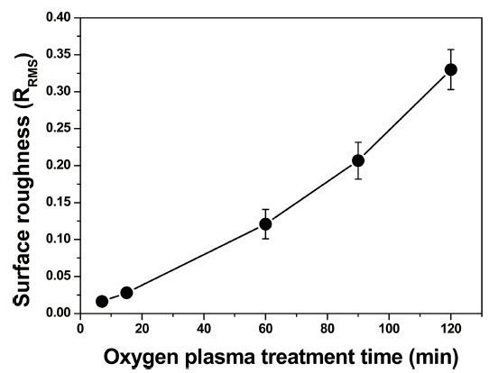
Fig. 2
Variation in the root mean square (RMS) surface roughness of the plasma-treated PET for different plasma treatment times.
As the authors showed in previous work,19) the peel strength at the Cu/PET interface increased in a stable manner with the plasma treatment time. However, there was a drastic increase after 60 min, reaching a peak value at 90 min, followed by a small decrease at 120 min.19) From the morphologies of the fractured Cu surfaces and cross sections of the fractured specimens after peel tests, it was found that the failure mode changed according to the plasma treatment time. Therefore, this study investigated the influence of the changed Cu/PET interface structures with plasma treatment time on the fracture mechanism of the Cu/PET flexible composite films.
Generally, PET is a semi-crystalline polymer with a transition temperature (Tg) of 61 ~ 81 °C, and its failure mode is the craze-crack mode.20-22) Tanrattanakul et al.23) explained that the failure of notched PET during tensile tests at a low extension rate (0.1 mm/min) occurred with the initiation and growth of a single thick craze at the tip of the core yielding zone of the notched PET, and then a crack propagated across the pre-existing craze. However, in this study, different crack propagation behaviors were observed depending on the plasma treatment time. This variation was thought to be related to the interface area between the Cu and PET, and to the width of the nanostructures formed on the PET surface.
Fig. 3 shows changes in the interface area between Cu and PET and the nanostructure width in the Cu/PET composite films [Fig. 3(a)], and the fracture mechanism of the Cu/PET composite film depending on the interface area [Fig. 3(b)]. Here, the interface area between Cu and PET was calculated by assuming the nanostructure shape to be a cone. As can be seen in Fig. 3(a), the interface area and nanostructure width increased smoothly until 60 min, after which they increased abruptly.
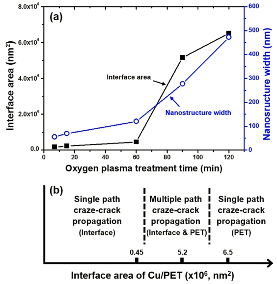
Fig. 3
(a) Changes in the interface area between Cu and PET and the nanostructure width in Cu/PET films fabricated by electroless plating after oxygen plasma treatment for different times. (b) Failure mechanism of the Cu/PET fillm depending on the interface area and nanostructure width.
From the fracture appearance shown in previous work19) and the change in the feature size of the nanostructure shown in Fig. 3(a), a failure mechanism of the Cu/PET composite film is proposed, as shown in Fig. 3(b). The variations in the failure mechanism can be explained in the following way. First, when the nanostructure size is small, i.e., the plasma treatment time is shorter than 60 min, as can be observed in Fig. 3(b), a single path propagation fracture mode is observed, where the crazecrack propagates in one direction along the interface between the nanostructure and the surrounding bulk PET. This fracture mode is caused by destruction of the small PET nanostructures under small stress. Because the Cu/ PET interface area and nanostructure width are small, only a small area of PET is supporting the applied load, as can be observed in Fig. 3(a). The reason the peel strength increases when the plasma treatment time was increased from 7 to 60 min is because there is an increase in the Cu/PET interface area and nanostructure width. Also, when the plasma treatment time was shorter than 60 min, craze fibrils,20-22) which are generally formed during the deformation and fracture of polymer, were observed,19) and the change in the size of the craze fibrils offers further insight into the increase in peel strength with plasma treatment time. The fibril size increased on the fracture surface when the plasma treatment time was increased from 7 to 60 min, which means that substantial energy was consumed during failure.
Second, when the interfacial adhesion of the 90 min plasma-treated Cu/PET increased, so that it became equal to the cohesive force of the PET itself, a multiple pass propagation fracture mode24) was observed [as shown in Fig. 3(b)], in which the craze-crack propagated in the PET layer surrounding the Cu/PET interface as well as in the interface between the nanostructure and the surrounding bulk PET.19) Because greater energy is required to fracture the Cu/PET due to multiple cracking, the Cu/PET has greater peel strength. Closer inspection of the fracture surface of the 90 min plasma-treated specimen (shown in Fig. 4) revealed the formation of several micro cracks in the Cu/PET interface and a crazing phenomenon that created pores during the tensile deformation of the polymer near the interface. This confirms a large amount of energy consumption.24)
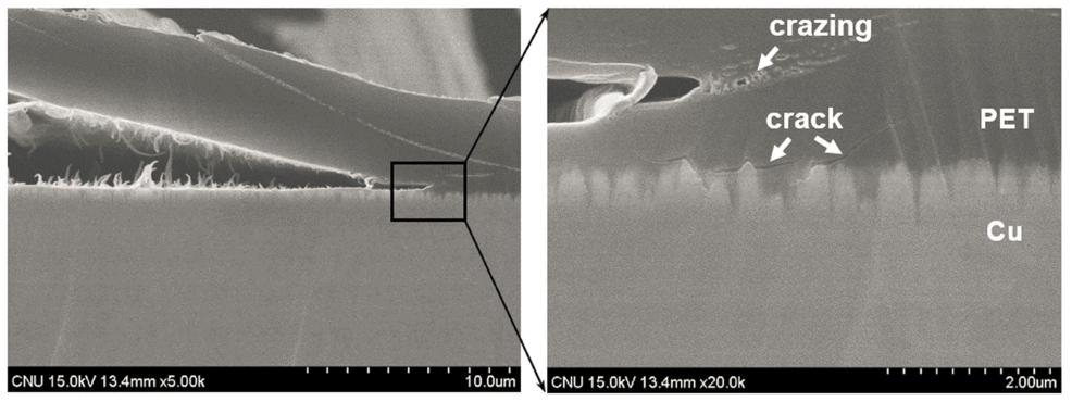
Fig. 4
Magnified SEM images of cross section of the fractured specimen after T-peel test of the Cu/PET fabricated by electroless plating after oxygen plasma treatment for 90 min. Multiple cracking took place near the Cu/PET interface, and new crazing and cracks were generating at high deformation region of crack tips.
However, when the Cu/PET interface area and nanostructure width increased, as in the 120 min plasmatreated specimen, the Cu/PET interfacial adhesion became greater than the PET cohesive force. This resulted in a single-path propagation fracture mode [as shown in Fig. 3(b)], during which the craze-crack propagated through the PET, rather than through the Cu/PET interface. Therefore, it was considered that the peel strength decreased because the energy consumption during crack propagation was less than that of the multiple-pass propagation fracture mode.
Fig. 5 presents SEM images of the fracture surfaces of the Cu layer and the PET layer on the fractured specimens after T-peel tests of the Cu/PET composite films, where the Cu-side and PET-side fracture surfaces were in contact with each other. The SEM images show the distinct difference in the fibrils’ size on the fracture surfaces, and the different propagation path of the craze-crack, which is further evidence showing the change in the Cu/PET failure mechanism according to the size of the nanostructure.
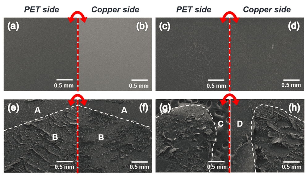
Fig. 5
SEM images of the fracture surfaces of the PET layers (a, c, e, g) and the Cu layers (b, d, f, h) on the fractured specimens after T-peel tests of the Cu/PETs fabricated by electroless plating after oxygen plasma treatment for 7 (a, b), 60 (c, d), 90 (e, f), and 120 min (g, h), in which the Cu-side and PET-side fracture surfaces are in contact with each other. The region ‘A’ refers to the fracture surface generated by the propagation of the craze-crack along the interface between the nanostructure and the surrounding bulk PET, and the region ‘B’ means the fracture surface generated by propagating the crack through the PET. C and D refer to the carbon tape used for SEM observation and PET free surface, respectively.
As can be seen in Fig. 5, the fibrils were very small in the 7 and 60 min-treated specimens, but their size increased significantly in the 90 and 120 min-treated specimens, indicating that the failure mechanism of the Cu/PET flexible composite film changed when the PET was plasma-treated for more than 60 min. In addition, even though the fibrils in the 90 and 120 min-treated specimens were similar in size, their crack propagation behaviors were different. In the 90 min-treated specimen, two different shapes of fracture surface were observed together as indicated by ‘A’ and ‘B’ in Fig. 5(e) and (f). Region ‘A’ refers to the fracture surfaces generated by the propagation of the craze-crack along the interface between the nanostructure and the surrounding bulk PET, which is similar to that shown in Fig. 5(a)-(d), while, region ‘B’ indicates the fracture surfaces generated by the craze-crack propagating through the PET. However, in the 120 min-treated specimen, only the fracture surface, such as that in region ‘B’ in Fig. 5(e) and (f), was observed. Fig. 5(g) and (h) shows that the craze-crack propagated through the PET, and then penetrated the PET surface. Therefore, the shape of the fracture surfaces shown in Fig. 5 well illustrates the change in the failure mechanism of the Cu/PET shown in Fig. 3(b).
Consequently, it was revealed that the failure mechanism of the Cu/PET flexible composite film varied depending on the Cu/PET interface area and nanostructure width. Thus, this work can provide a new design opportunity for wearable electronic devices with extended lifetimes, provided by excellent interfacial adhesion between copper and PET.
4. Conclusions
By observing the morphologies of the anisotropic nanostructures on plasma-treated PET surfaces, and the cross-section views and surfaces of the fractured specimens, it was revealed that the failure mechanism of the Cu/PET flexible composite film was dependent on the size and shape of the PET surface nanostructure (i.e., as determined by the plasma treatment time). When the interfacial adhesion showed a maximum (t = 90 min), a multiple pass propagation fracture mode was observed, where the craze-crack propagated in the PET layer surrounding the Cu/PET interface as well as in the interface between the nanostructure and the surrounding bulk PET. On the other hand, when the nanostructure size was smaller (t ≤ 60 min) or larger (t = 120 min), a single-path propagation fracture mode was observed. When the nanostructure size was smaller (t ≤ 60 min), the craze-crack propagated in the interface between the nanostructure and the surrounding bulk PET, and it propagated through the PET when the nanostructure size was larger (t = 120 min).
