

1. Introduction
2. Experimental Procedure
2.1. The theory part
2.2. The process of electrical conduction between extended states
2.3. The process of electrical conduction between localized states
2.4. Electric conduction (at Fermi level)
3. Results and Discussion
4. Conclusion
1. Introduction
Chalcogenide glasses are intriguing materials because of their excellent dependability for external applications and their simplicity in the near-infrared or visible regions as much as µm. Thermography is currently only performed using single-gem germanium (Ge), an interesting but expensive element.1) Ge alloys have been replaced by chalcogenide glasses in thermal imaging due to their lower cost and glassy nature, which allows for the molding of glass fibers due to their glassy nature.2) These days, infrared cameras typically use lenses with chalcogenide glass focus points, and the optical presentation of the framework is comparable to that obtained with Ge.3,4)
In optical fibers for light transmission, chalcogenide glasses made of Ge-Se alloys are frequently utilized, particularly when low length and adaptability are needed.5,6) The Ge-Se structure mainly includes Ge in the fourth coordination and selenium (Se) in the second coordination.7) Tetrahedral Ge is the basic building block of Ge-Se alloy, where Se chains or rings bond when 33 % Ge is added to Se.8,9) Ge-Se alloys are generally p-type but when mixed with plausible impurities such as lead (PbO),10) It can convert p-type conduction to n-type conduction.11,12)
Compared with the traditional p-n junction, the unique ability of these alloys to change from the p-type to the n-type (The transformation of the alloy from type p to n-type N results from a change in its composition, due to the disappearance of dangling bonds as a result of electron capture.) makes these alloys ideal materials for forming a p-n junction with many assembly advantages.13,14,15,16) Carrier-type reflectance (CTR) has been calculated in two series of Ge-Se-Pb glasses.17,18,19) In PbxGe42-xSe58 (x = 0~20), the CTR happens at x = 9 while in Pb20GeySe80-x (y = 20~22), the CTR happens at x = 21. Therefore, it makes sense that Ge-Se-Pb alloy will exhibit enhanced electoral qualities following CTR, the choice of lead element has the ability to form chemical bonds with the bonds dangling within the energy gap, which reduces randomness in the crystal structure. In addition, it is anticipated that the examination of the optical band hole in Ge-Se-Pb alloy following CTR will provide valuable information regarding the framework’s electrical characteristics.20,21)
This paper discusses the investigation of the temperature-dependent electrical characteristics of Se60Ge40-xBix glasses chalcogenides with varying concentrations (x = 0, 10, 15, and 20). To calculate the DC resistivity, conduction activation energy and electrical conductivity vs. temperature, the sample’s I-V as a function of temperature characteristics were noted. Furthermore, to compute the parameters that require it and ascertain the impact of the element’s partial replacement on the energy of extended and local states, constants like the energy gap were also computed.
2. Experimental Procedure
A bulk sample of chalcogenide glasses Se60Ge40-xBix (x = 0, 10, 15, and 20) of high purity (99.999 % purity) elements Se, Ge, and Bi were synthesized by melt quenching technique. For the sample compositions specified by (x = 0, 10, 15, and 20), the constituent elements were weighed according to their atomic ratios and each sample was placed individually in a quartz ampoule and sealed in ampoules under a vacuum of 10-4 Torr. After that, the sealed ampoules were put in a programmed furnace, controlled firunce, where the temperature was increased at a rate of 5 K per min up to 1,173 K and held at this temperature for 16 h. The sample fuse is then quickly quenched in cold water. Following that, the quartz ampoules were broken open to extract the samples from them. These alloys were then ground into a fine powder using a mortar and pestle and then reshaped into a pestle with radii of 15 mm and thicknesses ranging from 2 to 3 mm.
An ohmmeter was used to apply a voltage across the sample and measure the current through the sample because it has a built-in ability to output an independent voltage supply of 500 V. A locally designed sample holder with copper electrodes was used in the circuits for the bulk pellets. The basic circuit diagram used in this study is shown in Fig. 1. The electrical conductivity σDC was calculated from the relationship.20)
where, L is the thickness of the sample, R is the resistance of the sample, A is the cross-sectional area of the sample and ρDC are the resistivity of the sample under test.

2.1. The theory part
The charge transfer in amorphous materials is different from that in crystals. The high level of disorder in amorphous materials results in a wide distribution of bond angles, distances, and orientations. Whereas electrons migrating through crystallization experience periodic wells as much as possible, electrons migrating through an amorphous material experience a very inconsistent distribution of wells. This randomness in the crystal structure of materials leads to the emergence of multiple levels within the energy gap, and the density of these levels depends on the type of material and the amount of randomness in its crystal structure. Three types of states can be seen in the amorphous chalcogenides in the energy region between the bands. Whether it possesses external or intrinsic levels is of great importance.22)
The model of Cohen, Fritzche, and Ovshinsky (CFO)23,24) assumed that the non-crystalline structure would cause the band tails to overlap for the localized states as in Fig. 2(a). That derivative band of the conduction will be neutral when it is empty of electrons and the derivative of the band of valence is assumed to be neutral when filled with electrons. The region between the kinetic edge energies in conduction and valence bands is called a mobility gap. Mott and Davies proposed a neural model in which they strongly distinguish between local states that arise from the absence of a long-range system and those that result from structural defects.25,26) The first type the localized states extends only in the energy EA and EB in the mobility gap, as in Fig. 2(b).
The density of the defect states resulting from the longer tails is not high enough to maintain the Fermi level.25) To explain why the Fermi level is fixed and not displaced in glassy chalcogenides, the authors proposed the existence of local levels located near the center of the gap near the Fermi level, and these levels are local levels that are located above and below the Fermi level. They also suggested that compensation range states may act as deep donors and acceptors if they arise from defect centers such as dangling bonds. As a result, as shown in Fig. 2(c), the compensation range will be divided into the ranges Ey and Ex.

Fig. 2.
Band structure of amorphous materials showing the electronic state localized in the valence and conduction band tails. (a) Represents the overlap of valence and conduction tails as suggested by Cohen (CFO model), (b) Real density states gap (Mott-CFO model), (c) Same as (b) but with the compensation bands Ey and Ex.26)
Temperature-dependent electrical conductivity is widely used to investigate the conduction mechanism inside a material. As described by Davis and Mott, up to two mechanisms can control some semiconductors with random structure and in others up to 3- mechanisms can control the conduction of the electrons depending on how much or how little the crystal structure is random. The electronic conduction of random semiconductors can be described by the general Eq. (2).25,26)
where, (σ01, σ02, σ03) are pre-exponential factor parameters, (ΔE1, ΔE2, ΔE3) the activation energy of each term, KB is Boltzmann’s constant, are and T is the absolute temperature.
It can be concluded from Eq. (2) that the conductivity mostly depends on a variety of temperature ranges that the semiconductor is exposed. At lower temperatures, the electrical conductivity can be via electron hopping hole or electron between locations of localization energies state near the Fermi state. But at average temperatures, the electric conductivity of localization energy states appears at tails of energy bands, when electronic charges are transferred by jumps between local states in the region of tails of bands energy.
At elevated temperatures, electrical conductivity occurs between extended energy levels. The mobility, in this case, more than local state because there is a high density of energy states in the conduction and valence bands, so it is preferable to perform electrical measurements at elevated temperatures.23,24)
2.2. The process of electrical conduction between extended states
In the first region [the first term of Eq. (2)], and at high temperatures, the dominant mechanism is continuous electrical conduction across an extended state. Service carriers excited for extended states depending on activated energy ΔE1 where ΔE1 = EC − EF (or EF − EV).27,28)
where, N(Eext) is the density of extended state,22,23,24,25) is the electron frequency and inter-atomic distance there for the density of the extended state is calculated from Eq. (5).
The black arrow in Fig. 2(b) represents the excitation process. Which will be discussed later in the discussion and conclusion.
2.3. The process of electrical conduction between localized states
This conduction includes the second term of Eq. (2) when the glass alloy is exposed to chalcogenide at medium temperatures, inducing the second mechanism called local state conduction. In this case conductivity is arising from the tunnel through the states of unoccupied nearest adjacent centers.29) It was involving transport by electron or hole carriers on local states at band edge followed by hopping. Then activation energy is sufficient to move charge carriers across the edge of the beam tails EA and EB shown in Fig. 2 with the red arrow and the activation energy is ΔE2 = (EA − EF + w1) or (ΔE2 = EF − EB + w1) where w1 represented to activation energy for travel between local states.28,30)
where, Vph a phonon frequency = 1013 s-1, hopping distance between localize states R.22,23)
where, width of energy tail ΔE equal to (ΔE1-ΔE2) which shown in Fig. 2 and α- is coefficient of optical absorption is 10-7 cm.30)
2.4. Electric conduction (at Fermi level)
At lower temperatures, third conduction mechanism predominates by jumping between local levels at the Fermi level in the variable range (VRH).21) This type of tunneling involves charge carriers in a defect near Ex, Ey that varies with respect to the temperature range according to the following Eq. (10).28,30)
where, localization length of the gap states α-1 and N(EF) is the state density nears the Fermi level.27,28)
3. Results and Discussion
In order to systematically investigate the concentration dependence of bismuth in the Se-Ge-Bi glass system, four sets of glasses with distinctive features: Se60Ge40, Se60Ge30Bi10, Se60Ge25Bi15, and Se60Ge20Bi20 were prepared.
The electrical properties represented by electrical resistivity and continuous electrical conductivity were examined, and for the purpose of calculating the density of local and extended states within the energy gap, It will be applied the equations in the theoretical part to the electrical properties in order to extract electrical conductivity parameters.31)
Fig. 3 shows the temperature dependence of the constant electrical resistivity of four materials of Se60Ge40-xBix chalcogenides glasses at a different bismoth concentration (x = 0, 10, 15, and 20) with in a semi-logarithmic plot. A decrease in electrical resistance is observed with increasing temperature within the range (300 to 450 K). This is typical behavior of semiconductors. In addition, it can be seen from this figure that as the value of x increases, the electrical resistance decreases, and that there are two parts for each sample curve, which indicates the presence of two elements for resistance at temperature from 300 to 370 K and high temperatures (370~460 K).

Fig. 4 shows the variation of electrical conductivity with the formation of bismuth (Bi). It is noted from this figure that the four glasses Se60Ge40-xBix (x = 0, 10, 15, and 20) show a sudden increase in electrical conductivity with increasing Bi percentage. It can be observed that With every increase in the value of x, an increase in conductivity appears several times. This has been called a “surge” in conductivity. Two connection mechanisms are also observed in the temperature range (300~370 K) and (370~460 K).
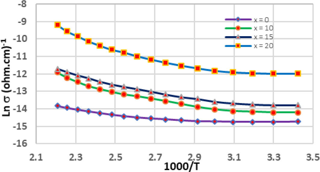
Eq. (2) shows that measurements of electrical conductivity in random semiconductors have 3 mechanisms: at high temperature (the extended state), at intermediate temperature (local states), and at low temperature (hopping between local states near the Fermi state). Sometimes a random semiconductor has two mechanisms, high temperature and medium temperature (conduction in localized states) and the absence of localized states at the Fermi level, and this applies to the results of our samples, so the third term is deleted from Eq. (2) and the equation becomes the Eq. (14).25)
In this section, the equations describing electrical conductivity are discussed in detail when the randomness of the alloy is low, i.e. based on Eq. (14), in which the conduction mechanisms are in the extended state and localized in the width of the tails only. To calculate the energy densities in the local extended state, the width of the tails (EA and EB). In addition to calculating the interatomic distance (a) and the hopping distance (R). We apply the equations derived in the theoretical part to the extracted results by drawing the relationship between the continuous electrical conductivity with temperature and represented in Fig. 4, which were collected and included in Table 1, for Se60Ge40-xBix chalcogenides glasses with a different Bi concentration (x = 0, 10, 15, and 20). It is noted from Fig. 2 that the alloys that were prepared do not have energy levels close to the Fermi level, as shown in Table 1. Therefore, the electrical conductivity of these alloys takes the path of Eq. (14), and this is confirmed by the results in Table 1, where it is noted that there are two values for the factor parameters. The exponents σ01 and σ02 that precede the exponent for each sample. For the purpose of calculating the conduction coefficients, we need Eq. (5) and Eq. (9) to calculate the energy state density for the local and extended states, respectively.
Table 1.
Electrical parameters in of Se60Ge40-xBix chalcogenides glasses at a different bismoth concentration (x = 0, 10, 15, and 20) at higher and lower temperature ranges.
| Compositions | ΔE1 |
σ0ext (Ω ‧ m)-1 | ΔE2 |
σ0ext (Ω ‧ m)-1 × 10⁻³ |
| Se60Ge40 | 0.857 | 128 | 0.44 | 74 |
| Se60Ge30Bi10 | 0.841 | 146 | 0.47 | 89 |
| Se60Ge25Bi15 | 0.794 | 165 | 0.42 | 99 |
| Se60Ge20Bi20 | 0.772 | 192 | 0.4 | 103 |
The interatomic distance (a) was calculated using the equation a = 0.026 e2/ℏ σ0ext,17) for all alloys listed in Table 1 and the values of (a) are listed in Table 2. It can be seen from Fig. 5 that the value of the interatomic distance generally increases with the increase in bismoth concentration, but from It is clear that the large increase when x = 20 is due to the spacing between the atoms, which led to a wider distance between the extended energy levels, which predicts a decrease in the density of bismoth.26,27,28,29,30,31,32)
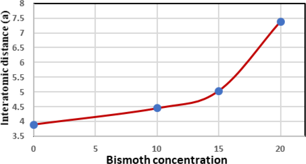
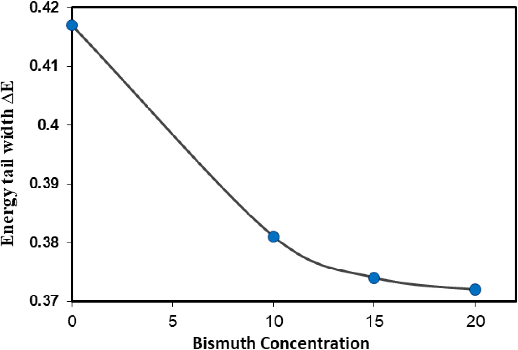
Fig. 6 represents the values of the energy tail width ΔE with the addition of bismuth to the Se60Ge40-xBix alloy. It can be observed that a decrease in the value of the tail width with increasing the concentration of bismuth in the alloy results in a reduction in the energy levels distance.33) It is clear that there is a significant decrease at concentration 20, and this indicates the convergence of atoms, which leads to a convergence of the distance between the extended energy levels, which predicts an increase in the density of the extended states.34,35)
Calculating the density of energy-extended states N(Eext) [conduction band extended density of states N(Ec) or valence band extended density of states N(Ev)] requires knowing the parameters of the exponential factor σ0ext, the tail width ΔE, and the atomic distance between atoms (a) from the equations in The theoretical part in each region and for each alloy is listed in Table 1 and these values are substituted into Eq. (5). The expanded state density was calculated and the results are listed in Table 2.
Table 2.
Tail width (ΔE), R, a, N(Eext) and N(Eloc) as function bismuth of Se60Ge40-xBix alloy with x = 0, 10, 15, and 20.
As for the density of local states, it was calculated from Eq. (9) after compensating for the values of both σ0loc and the jump distance (R). The relationship between the density of extended states of energy N(Eext) and the density of localized states was drawn in Fig. 7 with the concentration of bismuth, as it was observed from this figure that the density of extended states increases from 3.552 × 10²¹ to 5.86 × 10²¹ (ev-1 cm-3), As the concentration of bismuth increases from zero to 15, when the concentration of bismuth increases to 20, it becomes 5.864 × 10²¹ ev-1 cm-3. As for the density of local states, it decreases from 1.6 × 10¹⁴ to 4.2 × 10¹². This behavior indicates that increasing the concentration of bismuth has led to an increase in the regularity of the crystal structure of the samples and a decrease in the random structure.36,37)

4. Conclusion
In this manuscript, samples of Se60Ge40-xBix alloy with different proportions of bismuth were prepared using the molten point method. Continuous electrical tests were performed on the samples. Mathematical equations were applied and programmed to know the electrical conductivity mechanisms and electrical parameters, and to calculate the density of energy states on the continuous electrical conductivity results at different concentrations of bismuth, as well as the effect of partial replacement of elements. Electrical measurements revealed two conduction mechanisms: extended conduction at high temperatures and localized conduction at intermediate temperatures. Efficient substitution leads to a change in the local and extended state coefficients. It was noted that the best sample, Bi = 15, had the highest density of extended states and the lowest density of localized states, meaning that this concentration reduced the randomness of the crystalline structure of the sample, making it have more stable physical properties that contribute to electronic applications. The effect of activation energies, band tails, arid distance, and atomic distance as a function of concentration was calculated. It was found that all of these factors are significantly affected by the partial replacement of Ge with bismuth.
