

1. Introduction
Chemical vapor deposited(CVD) tungsten(W) has been widely used to fill small contact and via holes with a highaspect- ratio(HAR) in multilevel metallization of ultralarge- scale-integrated(ULSI) devices.1) The traditional Wplug deposition consists of three steps; silane (SiH4) pretreatment, W nucleation, and W-plug fill.2-4) Prior to SiH4 pretreatment, Ti/TiN is typically deposited as contact and glue/barrier layer. A SiH4 pretreatment is used to make a homogeneous and fast nucleation of W film on TiN.5) In addition, the SiH4 pretreatment could enhance the barrier performance of TiN by stuffing the grain boundaries with Si or SiHx.6) The SiH4 pretreatment is followed by the nucleation process, which traditionally involves the reduction of tungsten hexafluoride (WF6) by SiH4. The use of SiH4 in nucleation step ensures a fast nucleation and deposition of W on TiN with little incubation time and prevents the reaction of WF6 with Si or with the Ti contact layer. The third step, plug fill, is accomplished using H2 reduction of WF6. H2 is used for W-filling instead of SiH4 in order to give a conformal film with the lowest possible resistivity and particle levels.
It is generally accepted that the deposition of W nucleation layer using SiH4 reduction is a critical step in W-plug deposition because its conformality is relatively poor as compared to H2 reduction of WF6. For example, it shows adequate step coverages for larger features (> 80 % with opening diameters > 0.13 μm, 5:1 AR) but starts to degrade for narrower and higher-aspect-ratio features.7) Moreover, the requirement for W-plug deposition for evershrinking semiconductor devices described by international technology roadmap for semiconductors places more stringent demands on plug fill.8) In this respect, atomic layer deposition(ALD)9) is one of the most promising techniques to fulfill the above requirement. ALD-W films were deposited using disilane (Si2H6),10) SiH4,7,11-13) and diborane (B2H6)13) as reducing agents of WF6. Excellent step coverages at the HAR contact and via were obtained using ALD process. However, an ideally very low growth rate of 1 monolayer of W (~0.25 nm) per cycle10) as compared to that by conventional CVD can limit its applications in the semiconductor processing. In addition, the requirement of new deposition equipment for ALD process is another burden from the economical viewpoint.
Previously, we have reported the modified CVD-W nucleation process, called by pulsed CVD.14,15) Here, pulsed CVD is composed of 4 steps, resulting one deposition cycle: (1) Reaction of WF6 with SiH4. (2) Inert gas purge. (3) SiH4 exposure without WF6 supply. (4) Inert gas purge while the conventional CVD is consisted of the continuous reaction of WF6 and SiH4. By using this process, we could obtain a W nucleation layer with an excellent conformality at the HAR contact holes while still preserving a higher growth rate than that of conventional ALD. In this paper, we investigate the integration of pulsed CVD-W films as nucleation layers for W-plug deposition at DRAM technology. In this paper, the plug filling characteristics and contact resistance with pulsed CVD-W film as a nucleation layer were investigated and compared with conventional CVD-W nucleation process.
2. Experimental Procedure
Fig. 1 shows the schematic diagram of the sequence of pulsed CVD. The deposition stage of pulsed CVD is composed of 4 steps, resulting one deposition cycle: (1) Reaction of WF6 with SiH4. (2) Inert gas purge. (3) SiH4 exposure without WF6 supply. (4) Inert gas purge. In other cases, H2 could be added in the first and the third step. One of the stronger advantages of this process is the ability to use current CVD tools(Applied Materials Centura 5200 WxZ cold-walled and single wafer chamber) and process to successfully fill the ultrahigh aspect ratio contacts and vias. Detailed deposition conditions for pulsed CVD-W films were summarized in Table 1. For comparison, conventional CVD W films were deposited at a pressure of 30 Torr and susceptor temperature of 400 °C with 10 standard cubic centimeter per minute (sccm) of SiH4 and 50 sccm of WF6 gases diluted in Ar.
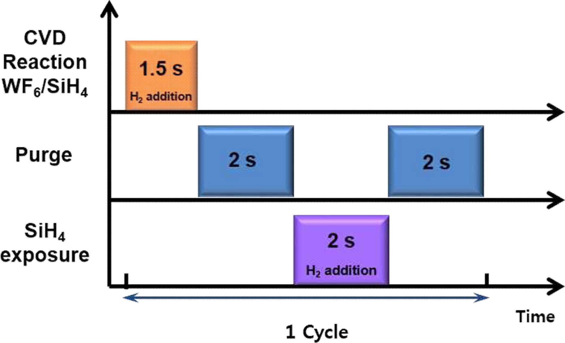
Table 1.
Summary of deposition conditions for pulsed CVD-W films.
| Sample I | Sample II | |
|---|---|---|
| 1st step | WF6: 30 sccm | WF6: 30 sccm |
| SiH4: 10 sccm | SiH4: 10 sccm | |
| H2: 1000 sccm | ||
| 2nd step | Ar/N2 purge | Ar/N2 purge |
| SiH4: 35 sccm | ||
| 3rd step | SiH4: 35 sccm | H2: 1000 sccm |
| 4th step | Ar/N2 purge | Ar/N2 purge |
In order to study the plug-filling characteristics and electrical properties, Si wafers were processed through DRAM process flow. The contacts connecting Al metal line with W bit line were patterned using ArF lithography and etched using high-density plasma. Then, to remove the thin oxide layer and surface etch damage, a deglaze step with 300:1 buffered oxide etchant(BOE) was carried out prior to Ti/TiN deposition. Ti glue layer was deposited into the contact by a biased ionized metal plasma(IMP) sputtering.16) And then, without breaking vacuum in an Applied Materials Endura chamber, 10-nm-thick TiN was deposited at 450 °C by thermal decomposition of tetrakis- (dimethylamido) titanium [TDMAT, Ti(N(CH3)2)4] with two periodic plasma densification steps for every 5 nm growth. Following the TiN deposition, W-plug process was performed. Blanket W deposition and etch-back were used to fill the contacts followed by metal line deposition. Here, W-plug deposition was composed of SiH4 pretreatment, pulsed CVD-W deposition as a nucleation layer, and W-plug fill at the deposition temperature of 400 °C using the same chamber. Finally, metal line patterning was accomplished. Contact resistances were measured using contact chain structures with two different contact sizes. Table 2 summaries the contact dimensions used in this study. Contact filling characteristics after W-plug deposition were characterized by plan-view scanning electron microscopy(SEM) operated at accelerating voltage of 200 kV(HD2000) after focused ion beam(FIB) cutting.
3. Results and Discussion
The systematic investigations on the properties of pulsed CVD-W films with deposition conditions have been described in details elsewhere.14,15) Here, we will point out the important findings. The pulsed CVD-W film had a much lower roughness (~0.7 nm at the thickness of ~20 nm) and better conformality at HAR contacts (AR: ~14:1, top opening diameter: ~250 nm, and bottom diameter: ~100 nm) as compared to that of conventional CVD-W nucleation layer deposited using WF6 and SiH4 as shown by Fig. 1.
Fig. 2 shows the resistivities of pulsed CVD-W films. It was found that film resistivities deposited by pulsed CVD were closely related with phases formed and microstructure characterized by grain size. For the sample I, the resistivity is as high as ~210 μΩ-cm. The high resistivity of sample I might be due to small grain size ranging from 5 to 11 nm and the formation of β-W phase with higher resistivity as compared to that of body centered cubic α-W. β-W films are reported to have significantly higher resistivity, as much as 150~350 μΩ- cm17) while α-W films deposited by CVD typically have a resistivity of ~20 μΩ-cm. H2 addition into the first and the third step (sample II) increased the grain size (11~ 18 nm) and prevented the film from forming an A15 β- W phase with a high resistivity, resulting in a film resistivity of ~100 μΩ-cm(Fig. 2). But, it is still higher than that of conventional CVD-W nucleation layer (~25 μΩ-cm).
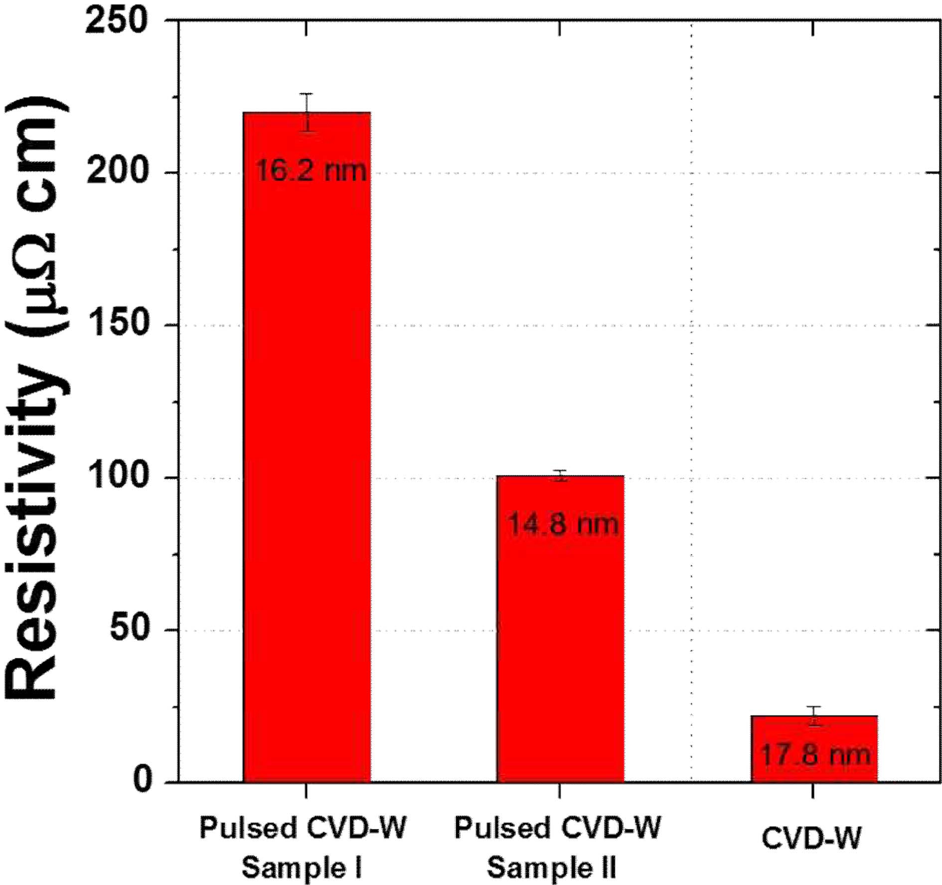
Fig. 3 shows the contact resistance distribution at the contact chains with different contact sizes. For contact chain A(Fig. 3(a)), a new scheme of pulsed CVD-W nucleation layer/W-plug fill shows a similar contact resistance compared with that of a conventional scheme of CVD-W nucleation layer/W-plug fill with the same thicknesses of nucleation layers. Considering a much higher resistivity of pulsed CVD-W nucleation layer, Fig. 3(a) indicates that the plug filling capability of the new Wplug scheme will be better compared to the conventional one. Fig. 3(a) also shows that the contact resistance decreases as the thickness of pulsed CVD-W film decreases. This is both due to the decrease in cross-sectional area occupied by pulsed CVD-W film with a high resistivity (~100 μΩ-cm) and the increase of cross-sectional area occupied by low-resistivity plug fill film (~15 μΩ-cm). The minimum thickness evaluated as a nucleation layer in this study was as thin as ~6 nm and the successful integration of this ultrathin nucleation layer indicates that pulsed CVD provides uniform nucleation and accurate thickness control like ALD process.
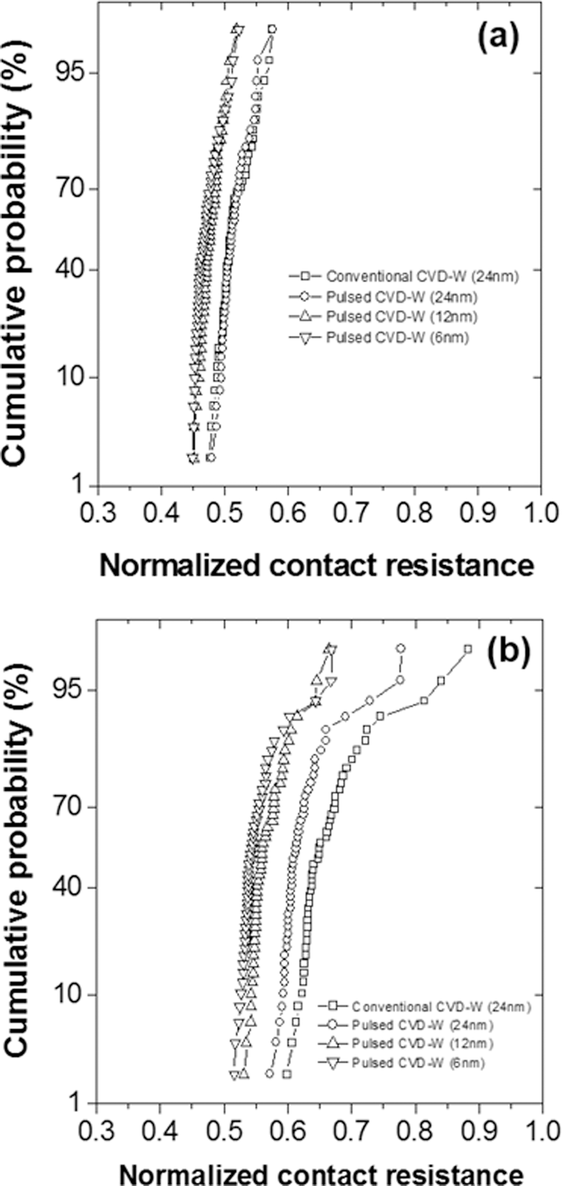
Fig. 3.
The distribution of normalized contact resistances at the contact chains connecting Al metal line with W bit line; (a) contact chain A and (b) contact chain B. Corresponding contact dimensions are summarized in Table 2.
As the contact size decreases(Fig. 3(b)), the new Wplug scheme of pulsed CVD-W nucleation layer/W-plug fill shows a contact resistance lower than that of conventional W-plug scheme even though the nucleation layers with the same thicknesses were applied. This indicates that the plug filling capability of conventional W-plug scheme is deteriorated with the reduction in feature size while the new one preserves its good filling capability. Fig. 3(b) also shows that the contact resistance can be lowered with a thinner nucleation layer, which is the same results with the case of larger size contact. Thus, it could be concluded that the pulsed CVD-W based plug fill scheme has a clear advantage with the reduction in device size.
Fig. 4(a) shows the plan-view SEM images of conventional W-plug scheme at contact chain B(see Table 2) after W-plug deposition. Twelve images were taken through the contact depths after precise cutting using FIB and thus, number 1 marked in the SEM image indicates the plug filling at the top of contact and 12 that at the bottom of contact. In Fig. 4(b), a schematic diagram for sample preparation and a typical FIB-XTEM image showing contact filling are provided. This technique is found to be successfully used for clearly observing the plug filling with contact depth at the very HAR contacts and vias even though the cross-sectional view observation fails to characterize the plug filing. As can be seen in Fig. 4(a), the conventional scheme has a large seam and this seam is formed through the bottom of contact. However, the drastically improved plug-filling capability of the new W-plug scheme is demonstrated as shown by Fig. 5. It is clear that the size of the seam at the same contact depth is significantly reduced and it disappears at the middle of contact. In the case of the new W-plug scheme, the seam in W-plug is mainly due to bowed contact profile not the conformality of nucleation layer. Fig. 6 showed the ratios of the area of the seam formed in the contact versus the cross-sectional area of the contact as a function of the contact depth [in fact, the positions SEM images were taken, which was shown at Fig. 4(b)] with W nucleation layer process schemes, based on Fig. 4(a) and Fig. 5. As expected, the ratio was always higher for the W-plug formed by a conventional CVD-W nucleation process/W-plug fill irrespective of the contact depth as compared to that for the one by a new W-plug process using a pulsed CVD nucleation layer (sample II). It was already reported that the step coverage of the pulsed CVD-W nucleation layer was superior to that of the conventional CVD-W nucleation layer.14) And, from Fig. 6, it is apparent that the improved step covearage of the nucleation layer resulted in the improved W-plug film. Thus, it can be deduced that a lower contact resistance of the new W-plug scheme of pulsed CVD-W nucleation/W-plug fill is mainly due to the excellent filling capability at the very small-sized contacts considering the most of contact was consisted of the Wplug fill not the nucleation layer.
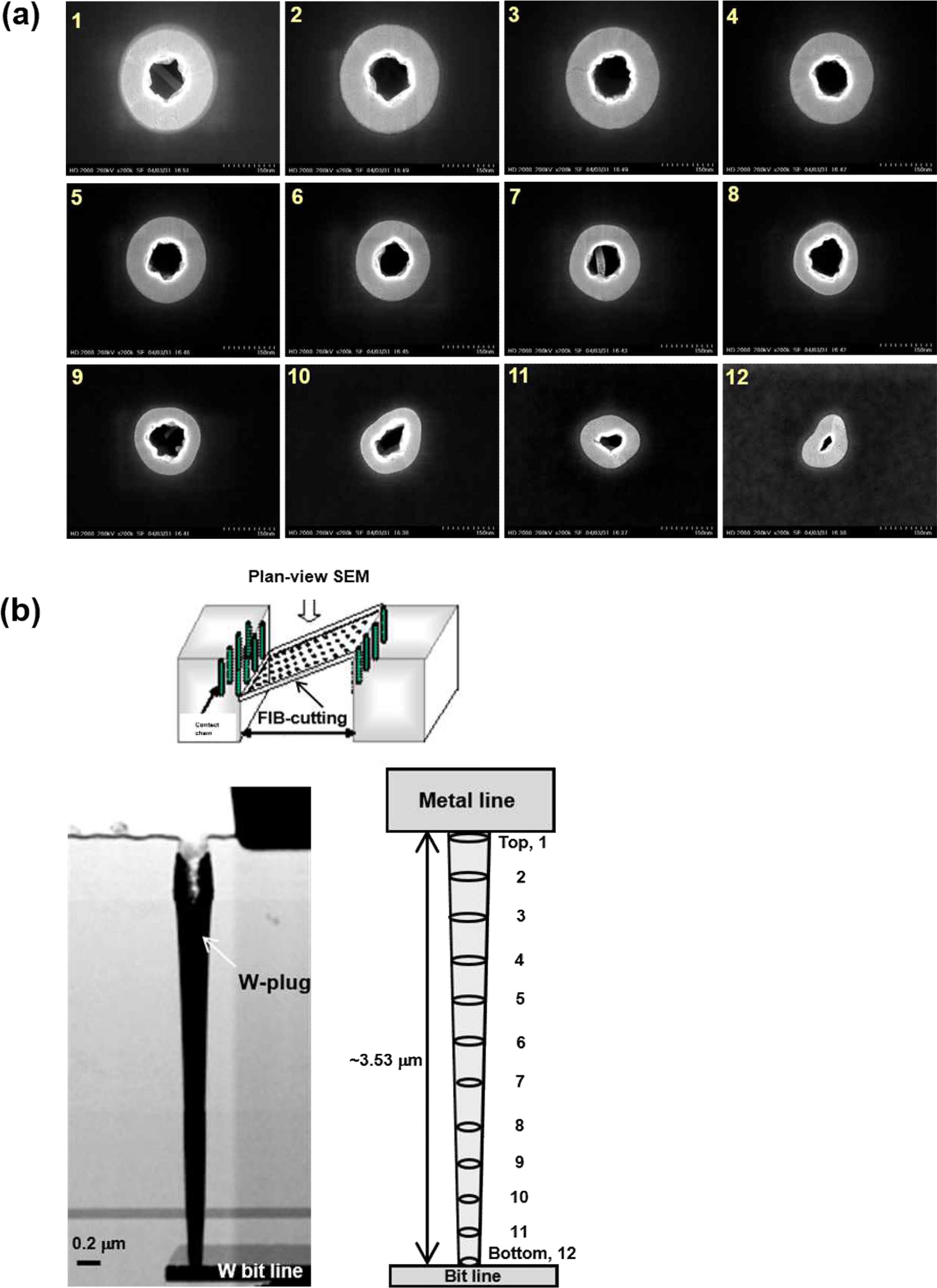
Fig. 4.
(a) The Plan-view SEM images of conventional CVD-W nucleation layer/W-plug fill scheme at contact chain B with contact depths and (b) the schematic diagram for sample preparation using FIB-cutting and typical FIB-XTEM image showing contact filling. 1 marked in the Fig. 5(a) indicates the plug filling at the top of contact and 12 that at the bottom of contact.
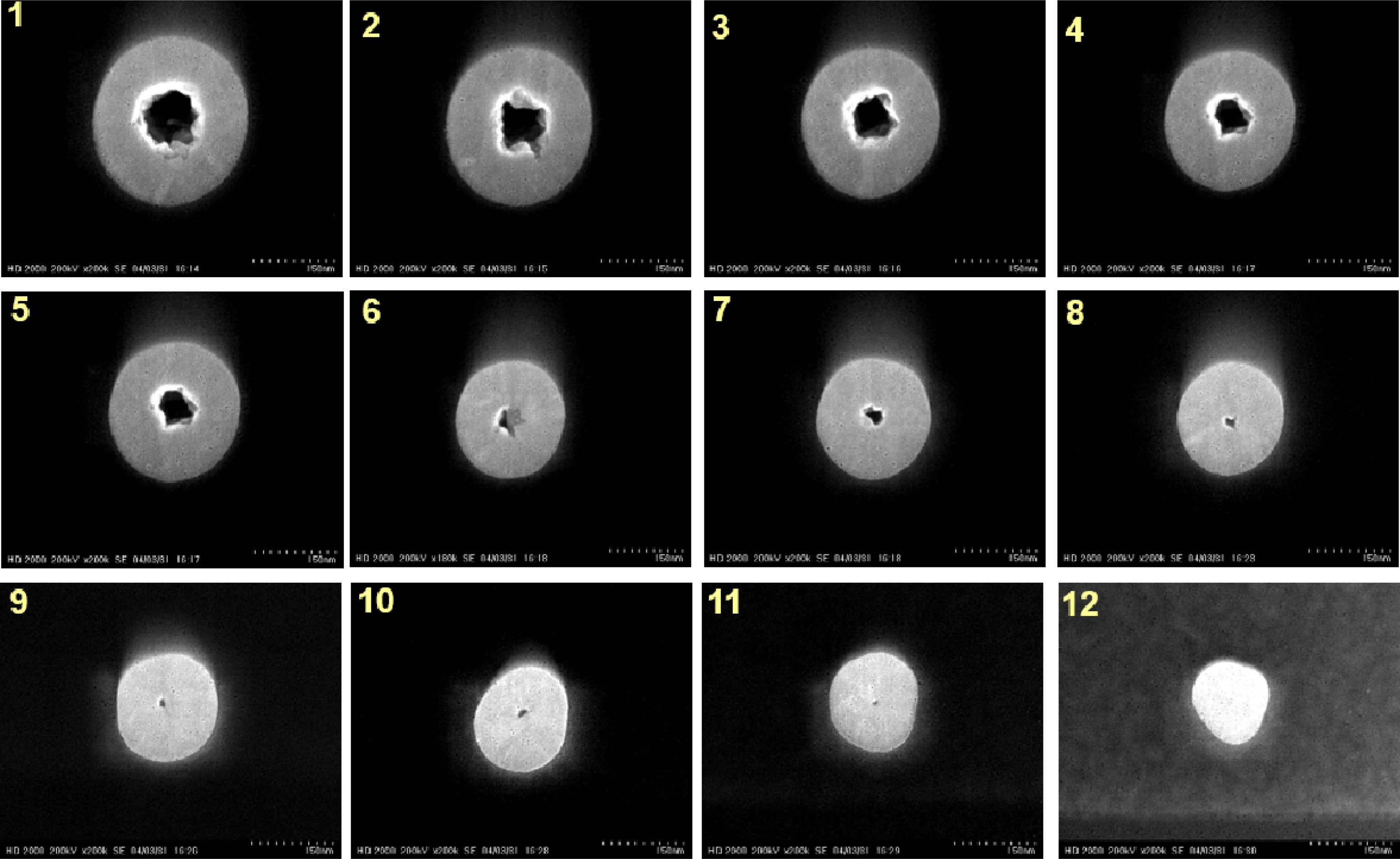
Fig. 5.
The Plan-view SEM images of pulsed CVD-W nucleation layer (sample II)/W-plug fill scheme at contact chain B with contact depths.
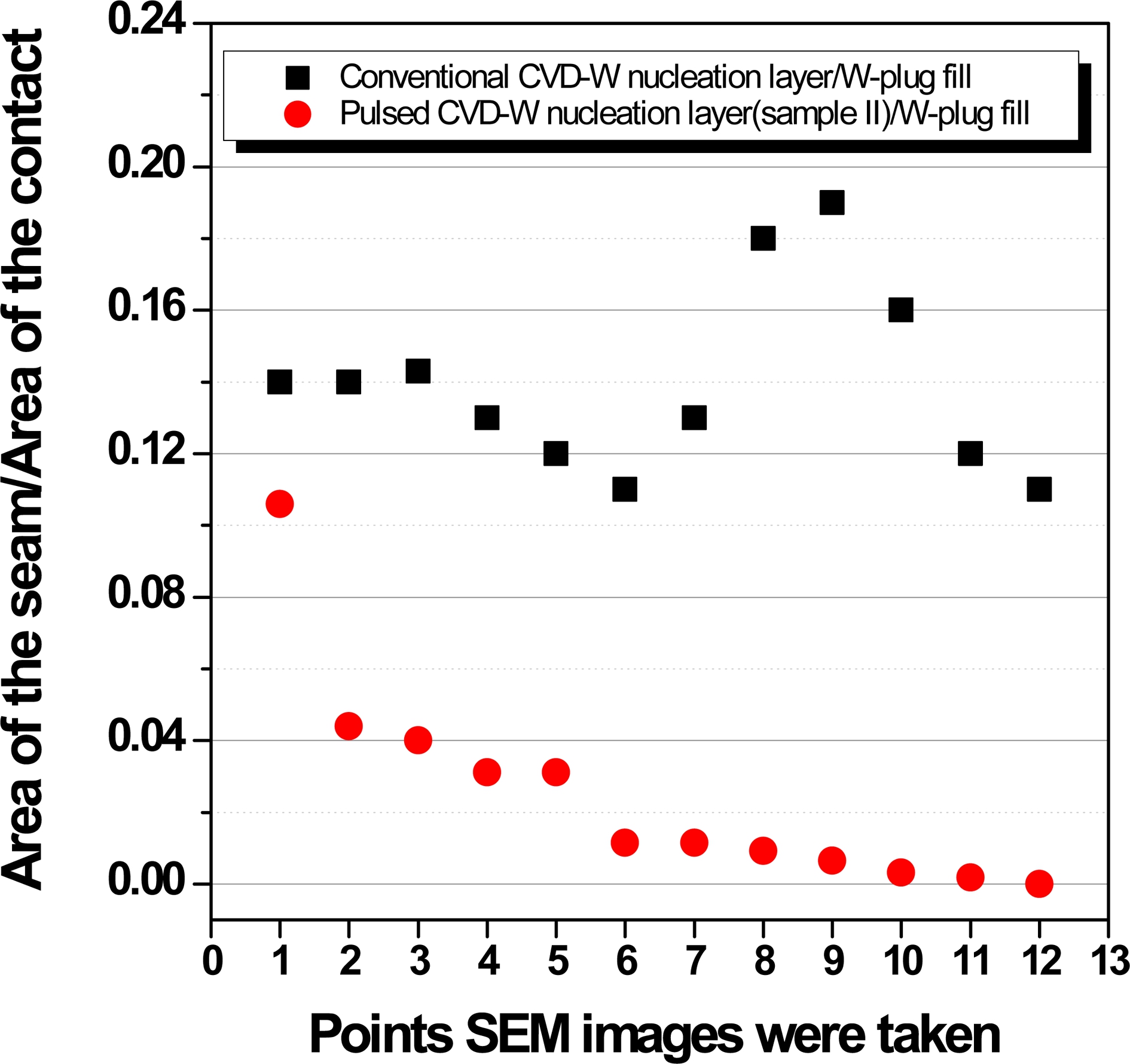
Fig. 6.
The ratio of the area of the seam formed in the contact versus the cross-sectional area of the contact as a function of the contact depth, which was calculated considering Fig. 4(a) and Fig. 5. In fact, the x-axis of the graph indicated the points SEM images were taken, which was shown at Fig. 4(b).
In the case of W-CVD using SiH4-chemistry, it is well known that the step coverage of W film is mainly degraded by the decrease of SiH4 concentration at a deep contact hole due to its lower diffusion coefficient and higher reaction order as compared to H2-chemistry.1) As can be seen in Fig. 4(a), the poor step coverage of nucleation layer could lead to a large seam in the final plug fill. This may become open after subsequent planarization processing such as etch-back or chemical mechanical polishing, which increases the contact and via resistance and degrades the quality of contact and via. However, in the case of pulsed CVD, both purge step using inert gas and SiH4 exposure step provided sequentially after a short CVD reaction prevented the reactant starvation at HAR contact hole, resulting in improving the film conformality. Moreover, the addition of H2 in the precursor pulsing and reactant pulsing step (sample II) could improve the step coverage of pulsed CVD-W film further. The improved conformality of nucleation layer leads to the excellent W-plug filling.
4. Summary and Conclusions
In summary, thin and conformal W nucleation layer is critically necessary for successfully filling the ultrahighaspect- ratio small plug as the device is ever-shrinking. In this study, we have demonstrated the new W-plug integration scheme to use pulsed CVD-W film as a nucleation layer. Pulsed CVD process has a strong advantage that it successfully fills the HAR contacts and vias using the current CVD tools. The results showed that pulsed CVDW based plug fill scheme showed a lower resistance at the contact holes of DRAM as compared to conventional CVD-W based one. A novel characterization technique using FIB cutting clearly showed that a drastically improved plug filling was achieved by employing pulsed CVD-W film. Improved filling was thought to be due to the excellent step coverage of nucleation layer deposited by pulsed CVD. One of important findings in this study is that the pulsed CVD-W based plug fill scheme has a clear advantage due to its better plug-filling capability as the contact dimension is reduced. Thus, it could be concluded that pulsed CVD-W process can be considered as one of the possible solutions to deposit a very thin W nucleation layer for future DRAM W-plug process.
