

1. Introduction
The structural and optical properties of zirconia have a great influence on the performance of devices that are used in the different fields of technology.1,2) These properties are greatly altered by various parameters such as pH of the electrolyte, the concentration of the electrolytic solution and heat treatment.3) Thermal annealing is one of the crucial aspects to boost the stability and efficiency of photosensitive devices.4) Zirconium oxide thin films (ZrO2), also known as zirconia, are one of the transition metal oxides with outstanding physical, optical and chemical properties including transparency in visible as well as near-infrared regions, high refractive index and large optical bandgap.5-11) ZrO2 normally exists in three natural phases: monoclinic, tetragonal and cubic at different temperatures.12) The tetragonal phase is reported to be suitable for optoelectronic applications as insisted by various studies.13-15) The tetragonal phase can be stabilized at low annealing temperature with the variation of hydrolysis catalyst.16) The monoclinic to tetragonal transformation commonly develops in the course of sintering and on both heating and cooling, which is the issue of extra vigilance.12) Pure zirconia inevitably disintegrates by cracking due to extensive internal stress developed on the cooling of sintered specimen. To sustain the integrity of zirconia at room temperature, one can either stabilize the tetragonal or cubic phase by alloying or by annealing it at low temperature, which leads to high toughness and strength of ceramic material. This mesoporous material has opened several new avenues in research owing to its controllable pore size, easy functionalization17) and large surface area. The phase structure of ZrO2 greatly influences its physical and chemical properties, which directly depend upon the time and temperature of annealing. The residual stress, which depends on the deposition rate and deposition temperature, is shown to play an important role in the variation of microstructure. Post annealing treatment and elevation of deposition temperature are found to be one of the simplest ways of crystallizing thin films.18) Annealing temperature not only modifies the morphology and size of nanoparticles but also affects the defect states and thus reconstructs energy levels. Furthermore, annealing temperature customizes the phase of the materials, thereby affects their structural and optical properties. Thus, studies regarding the effect of thermal annealing on structural and optical properties of thin films are very important to understand for the enhancement of device performance in different fields.19) As the structural and optical properties of thin films can be affected by some factors such as the deposition method, the deposition conditions and thermal annealing, this investigation focuses on the influence of annealing time on structural and optical characteristics of ZrO2 thin films. So, in present paper the effect of annealing on morphology, crystallinity, transmittance and energy band gap of pure and nickel doped ZrO2 films are presented and discussed.
2. Experimental Procedure
Homogeneous solutions of pure and nickel doped ZrO2 (0 %, 1 % and 5 %) have been synthesized by the sol-gel method. Zirconium oxychloride octahydrate (ZrOCl2·8H2O), nickel chloride hexahydrate (NiCl2·6H2O) was used as starting material for the synthesis of sols. 2-butanol and ethanol were mixed in equal volumetric ratios to dissolve the material’s salt. The procedure of preparing un-doped ZrO2 is already available in previous studies.20,21) O nethird of this mixture was employed to dissolve zirconium oxide salt and the remaining mixture for nickel salt. Oxide solution was stirred for 60 minutes and then nitric acid as an oxidation agent, acetylacetone as a stabilization agent and water for hydrolysis were added into the solution having a ratio of 0.4 : 5 : 15. Afterward, nickel solution having the prescribed concentration i.e. 1 % and 5 %, was added slowly into the oxide solution followed by continuous stirring for the next 100 minutes till a clear solution was formed. Firstly, four samples of pure ZrO2 were synthesized for the calibration of the time of annealing appropriate for structural study. Subsequently, to check the annealing effect, eight films (four on glass substrates for structural characterizations and four on quartz substrates for morphological and optical characterizations) have been prepared from each solution i.e. pure ZrO2, 1 % Ni-ZrO2 and 5 % Ni-ZrO2, by sol-gel dip-coating technique. To gain sufficiently thick films for XRD analysis, the procedure of dipping and drying was repeated 10 times on glass substrates. Two films, one from glass and one from quartz substrates from each solution are kept without heat treatment (as-deposited) for further characterizations. Out of six remaining films from each solution, two films (one on glass and one on quartz substrate) are annealed at 300 °C, two films at 400 °C and two films at 500 °C. Scanning electron microscopy, X-ray diffraction and UV-visible spectroscopy were employed to study the morphological, structural and optical characterizations of synthesized films at different annealing temperatures.
3. Results and Discussion
3.1. Morphological and Elemental Analysis
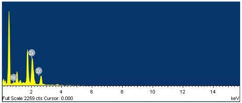
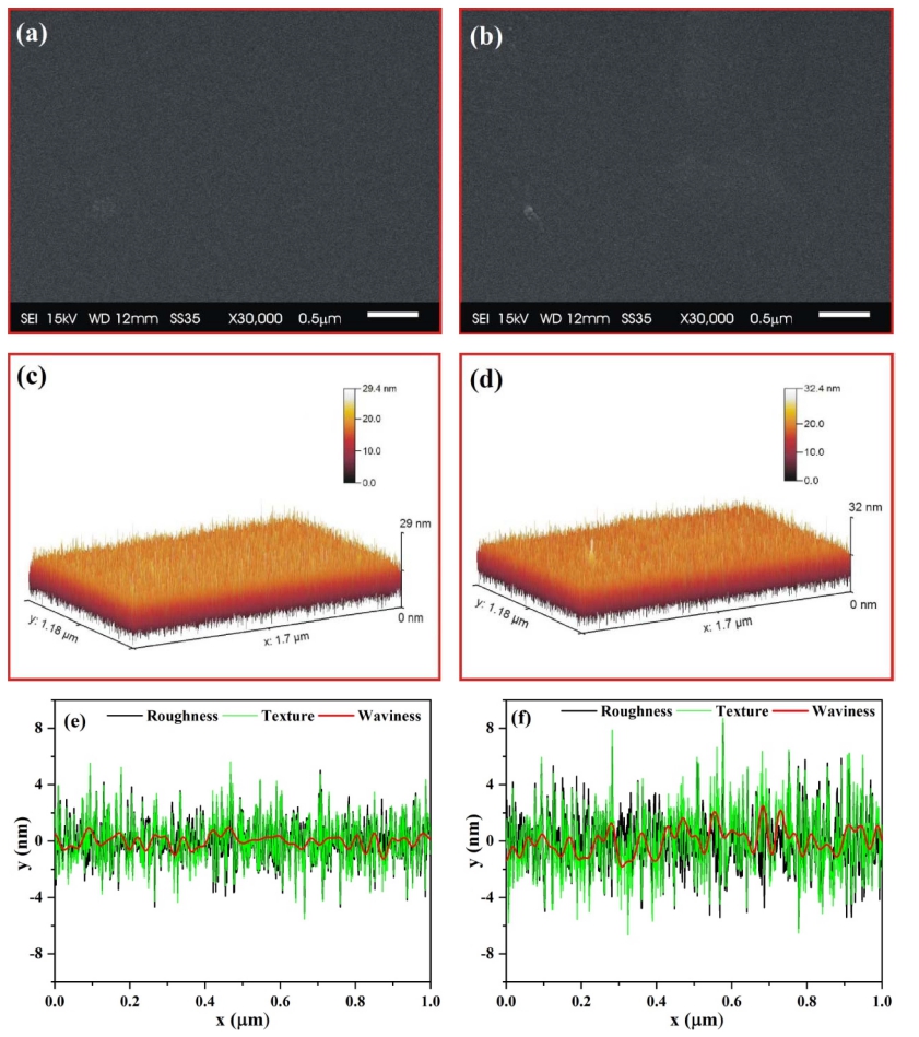
Fig. 1 represents the EDS spectra of 1 % nickel-doped ZrO2 thin film deposited on a glass substrate. The exact quantity of nickel can’t be estimated due to the presence of silicon and oxygen in the glass substrate, although it's doping in the ZrO2 can be confirmed by EDS spectra. Fig. 2 represents the surface analysis of as-deposited and annealed 1 % nickel-doped ZrO2 films. Figs. 2(a) and 2(b) represent the surface morphology for as-deposited and annealed films respectively, which is recognized to be smooth for synthesized films. SEM micrographs are analyzed through ’Gwyddion software’ to get clear information regarding surface roughness parameters.22,23) Figs. 2(c) and 2(d) represent the 3D view for the as-deposited and annealed film. Variations of roughness parameters i.e. roughness, texture and waviness are presented in Figs. 2(e) and 2(f). The average roughness and waviness of as-deposited film were evaluated to be 1.02 nm and 0.34 nm, which is smaller as compared to the annealed film i.e. 1.63 nm and 0.68 nm respectively. The increase in surface roughness on annealing the film is due to the agglomeration of grains with increasing temperature and is found to be in good agreement with existing literature.24)
3.2. Structural Analysis
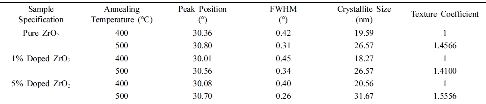
Fig. 3(a) shows the XRD patterns of pure ZrO2 films annealed at different temperatures for two hours. Amorphous nature was observed for as-deposited and 300 °C annealed films due to the absence of diffraction peaks in the XRD spectra. Starting of crystallization was recorded for the film annealed at 400 °C because of the presence of a diffraction peak located at 2θ value of 30.36°. Increase in crystallinity was detected due to the generation of four crystallization peaks with the upsurge of temperature to 500o at 2θ values of 30.80°, 35.49°, 51.08° and 60.62° having tetragonal orientation along (101), (110), (112) and (211) planes. Fig. 3(b-c) represents the XRD patterns of as-deposited and annealed films for 1 % and 5 % nickel-doped ZrO2 thin films. As seen for pure ZrO2 in Fig. 3(a), a similar trend of diffraction peak was observed for 1 % and 5 % nickel-doped ZrO2 thin films. No diffraction peak resembling nickel lattice is observed for both the doped films. The diffraction peaks turn narrower and intensified with annealing, resulting in enhancement of crystallinity. The reduction in the FWHM of the diffraction peaks with the increase of the annealing temperature is ascribed to the coalescence of grains at higher temperatures.25) The intensity of peaks for 5 % nickel doped films annealed at 500 °C, slightly decreased as compared to the pure and 1% doped specimen and the peak assigned for (110) is almost diminished as can be seen from Fig. 3(c), which might be due to the change in point defects and electron density.26)
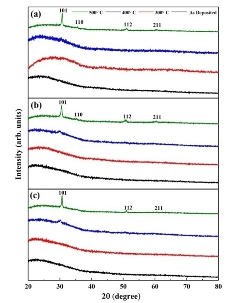
Fig. 3
XRD pattern of (a) pure (b) 1% and (c) 5% Ni-ZrO2 thin films annealed at different temperatures.
Crystallite size of nanocrystalline ZrO2 films is calculated from the full width at half maximum (FWHM) of the most intense peak by Scherrer’s formula27) given in Eq. (1).
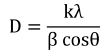
Where D is the crystallite size, k is the numerical constant (taken as 0.9), λ is the wavelength of the incident light, β is full width at half maximum and θ is Bragg angle. All the deposited films are found to exhibit broader diffraction peaks as compared to standard XRD data, implying toward smaller crystallite size of the synthesized films. Crystallite size is found to increase with the increase in annealing temperature as mentioned in Table 2. Increase in crystallite size during annealing points toward the propensity of large grain growth in the films that pursue as a result of displacement of atoms to the appropriate positions to merge into adjacent particles constituting larger particles due to heat treatment.28)
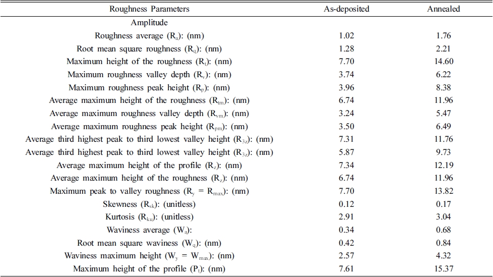
Table 2
Variation of structural parameters of pure, 1 % and 5 % nickel doped ZrO2 thin films with annealing temperature.
 |
For attaining the quantitative information regarding the preferential crystalline orientation of synthesized films, texture coefficient (TC(hikili)) was calculated by Barret and Massalski relation29) also known as Harris’s formula30) given by Eq. (2):
Here I0(hikili), and I(hikili) are the integrated intensity ratios of thin films and bulk randomly oriented ZrO2 powder respectively and n is the number of diffraction peaks. The departure of texture coefficient from unity represents the degree of preferred orientation along a particular diffraction plane as compared to bulk respectively. Results of texture coefficient calculations revealed the high orientation of synthesized films toward the (101) plane, however, the value of TC(hikili) = 1 represents the randomly oriented crystallites in the film [31].
3.3. Optical Analysis
Fig. 4(a) represents the UV-visible spectra and equivalent inset CIE chromaticity diagram of as-deposited and annealed samples at different temperatures for pure ZrO2 thin films. Average optical transmittance was found to vary from approximately 80 to 95 % from room temperature to 500 °C in the wavelength range of 250-700 nm. Absorption of light below 250 nm is due to the stimulation of electrons from the valence band (VB) to the conduction band (CB) of ZrO2. High transmittance was observed for the as-deposited film, however, the annealing of films represents a slight decrease in transmittance with the increase in annealing temperature. This phenomenon is assigned to the light scattering effects due to the increase in roughness with the increase in annealing temperature.32)
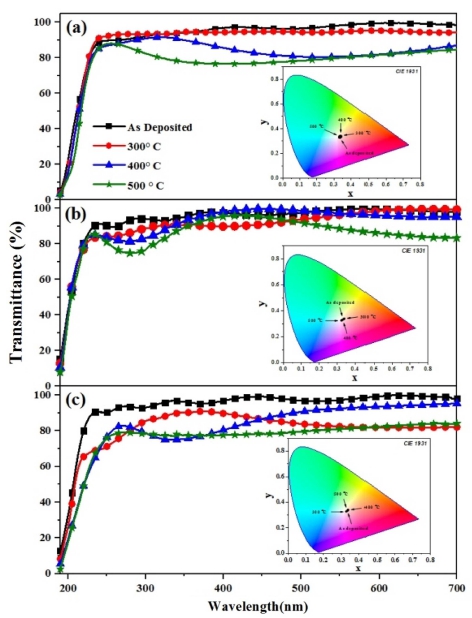
Fig. 4
UV-Visible transmittance and CIE chromaticity (inset) of (a) pure (b) 1% and (c) 5% Ni-ZrO2 thin films annealed at different temperatures.
Fig. 4(b-c) represents the UV-visible transmittance spectra and corresponding CIE chromaticity diagram of 1 % and 5 % nickel doped ZrO2 thin films without annealing and annealing at different temperatures. A similar trend of decrease in transmittance with the increase in annealing temperature was observed as already seen in the case of pure ZrO2 thin films. In addition, transmittance also decreases with the increase in the crystallinity of the material. Crystallite size decreases with the decrease in the crystalline phase due to the increase in the degree of disorder, which leads to a decrease in optical absorption.
The optical band gap of synthesized films was evaluated by Tauc’s plot using the relationships33,34) given by Eqns. (3) and (4):
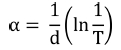
Here a is the absorption coefficient, β is the constant, hv is the photon energy and n denotes the type of transition (for direct gap transition n = 2) and Eg is the bandgap. The energy bandgap is observed to decrease with the increase in annealing temperature in the range of 5.74 - 5.51 eV, 5.96 - 5.80 eV and 5.86 - 5.33 eV for 0 %, 1 % and 5 % nickel doped films respectively as described in Fig 5. Decrease in bandgap energy with an increase in temperature is attributed to the expansion of crystal lattice and weakening of the inter-atomic bonds.35,36) Weaker bonds signify that less energy is required to break a bond and bring an electron into the conduction band. So, it is apparent that the energy band gap decreases with the increase in annealing temperature as discussed in existing literature.37,38) The variation range of bandgap is broader for 5 % nickel doped films as compared to 1 % doped films due to the formation of larger crystallites at high doping percentage due to agglomeration of grains around the dopant material as mentioned in Table 2. In addition, the optical band gap decreases with the increase in the percentage of crystalline phase in the material, as was also discussed by C. Rotaru et al.39) in his comparative study of amorphous versus crystalline silicon.
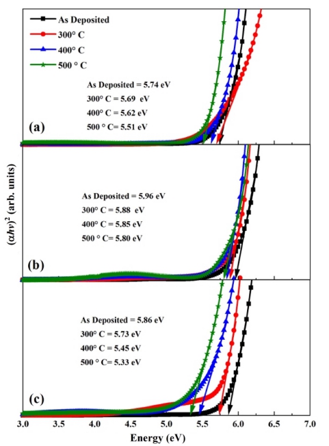
Fig 5
Energy band gap of (a) pure (b) 1% and (c) 5% Ni-ZrO2 thin films annealed at different temperatures.
Extinction coefficient (k) can be calculated by Eq. (5) given as follows40)

Fig. 6 represents the wavelength dependence of extinction coefficient of pure and nickel doped films annealed at different temperatures. It is observed that the extinction coefficient increases in the wavelength region of 250 - 700 nm with the increase in annealing temperature. This behavior of extinction coefficient with the increase of annealing temperature proves that the fraction of light loss due to the scattering process increases with the increase of annealing temperature.41)
Fig. 6
Extinction coefficient of (a) pure (b) 1% and (c) 5% Ni-ZrO2 thin films annealed at different temperatures.
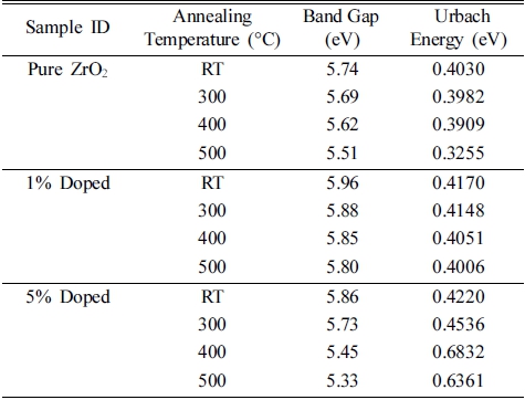
Urbach or band tail energy (Eu) of as-deposited and annealed films was calculated with the help of Eqs. given by42)
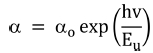
Fig. 7 illustrates the plots of ln(a) versus incident photon energy (hv) for pure and doped ZrO2 films and values of Eu are tabulated in Table 3. Eu was found to decrease with the increase in annealing temperature for pure and 1 % nickel doped ZrO2 films as mentioned in Table 3. Decrease in the Urbach energy values with the increase in annealing temperature points toward the decrease in localized states representing a correspondence with XRD results (Fig. 3) demonstrating the increase in crystallinity.43) This tendency proves that the degree of structural disorder decreases with the increase of annealing temperature up to a certain point. Afterward with the increase of annealing temperature the Urbach energy increases for 5 % nickel doped ZrO2 films. Thus, the distortion of the crystal structure of the film at a high concentration of nickel occurred, which may be due to the oxide formation, thereby causing the sudden increase of Urbach energy up to the certain limit of annealing.44) However, at 500 °C of annealing temperature, high crystallinity is responsible for the decrease in Urbach energy as was seen for 1% nickel doped films (ref. Table 3).
4. Conclusions
Transparent thin films of pure and nickel doped ZrO2 were synthesized by the sol-gel dip-coating method at different annealing temperatures. The surface morphology of the as-deposited film was found to be smoother as compared to annealed films due to the agglomeration of grains and crystallization of film at high temperatures. An increase in the values of surface texture parameters i.e. roughness and waviness ensures the decrease in surface smoothness with the increase in annealing temperature. EDS spectra certify the nickel doping in as-deposited as well as annealed ZrO2 films. Thin films of pure and doped ZrO2 deposited at room temperature and annealed for two hours remain amorphous up to 300 °C of annealing temperature. One crystallization peak was observed for all the films annealed at 400 °C. Four crystallization peaks have been detected for the film annealed at 500 °C with a tetragonal orientation. All the crystallized films were highly textured along the (101) plane. UV-visible results revealed high transparency of about 80 to 95 % for all the deposited films. The highest transparency was recorded for the as-deposited film, which decreases with the increase in annealing temperature due to the increase in light scattering effect. The optical band gap was observed to decrease from 5.74 - 5.51 eV, 5.96 - 5.80 eV and 5.86 - 5.33 eV due to an increase in crystallinity with the increase in annealing temperature for 0 %, 1 % and 5 % nickel doped films. Urbach energy (Eu) was in good agreement with the crystallinity of films and was found to decrease with an increase in annealing temperature. However, the key conclusion can be considered related to the high transparency and smoothness of films due to which these films can be used in the coating of optical devices where high transparency to the visible light and smoothness of the surface is the prime requirements.
