

1. Introduction
Porcelain insulators have been widely used to mechanically support and electrically insulate transmission lines.1) The insulators occupy a small fraction of the cost of the construction of power transmission system, but they play a very important role in the reliability of transmission lines and can account for large part of the failure and maintenance of the lines.2-4)
For many years in service, the aged porcelain insulators are exposed to continuous environmental, mechanical, and electrical stresses, which include flashover, wind, rain, ice, salt water, etc..5-7) These stresses can lead to the formation of defects, degradation of electrical performance, and the reduction of mechanical strength, which can result in mechanical and electrical failure.8-12) And so, the replacement strategy of aged porcelain insulators is very important. The best-case scenario is the replacement on the day before failure, which is practically very difficult and also risky. This is why the appropriate estimation of the lifetime of aged porcelain insulators is highly desired. Accurate methods to evaluate the degree of degradation are needed to determine the remaining lifetime. Human eyes and several equipment such as UV, IR, and night vision cameras have been widely used to observe the pollution, electrical/mechanical failure of the insulators. 13-16) These methods, however, can only detect the contaminants on the surface and the corona discharges of the porcelain insulator, and it is difficult to detect cracks existing in the interface or inside of the insulators. The microcracks inside the insulator can propagate under stress, which can lead to the decrease of electrical and mechanical strength.8) Metallography techniques such as optical microscopy(OM) and scanning electron microscopy (SEM) have been used to observe the internal microstructure of the materials.17-19) Metallography can see the nanoscale defects directly. But it needs preparation of a very smooth sample surface before observation, has the disadvantage of being destructive and can only observe a small portion of the material. On the other hand, the Xray 3D computed tomography(CT) can be used to obtain the number, size and spatial distribution of the defects without the need to destroy the material to prepare a very smooth sample surface. It, however, is an indirect analysis method, and so it can have problems related to the reliability. If both metallography techniques and Xray 3D CT are appropriately used, it is expected that the internal defects of aged insulator can be effectively observed, which can improve the accuracy of the prediction of degradation and the evaluation of lifetime, but detailed studies using X-ray 3D CT have not been reported.
In this study, the microstructure, phase and mechanical properties of three aged porcelain insulators which were manufactured in different years(1973, 1995 and 2008) and which were used in the field for different amount of time, were investigated in order to find out the possibilities of using the information from the X-ray 3D CT to help improve the accuracy of the prediction of the degradation and the evaluation of lifetime. The information on distribution and size of defects within the aged porcelain insulators was obtained by X-ray 3D CT, OM, and field-emission SEM(FE-SEM). X-ray powder diffraction(XRD) was used for the qualitative and quantitative phase analyses. The amounts of defects and phases of the three porcelain insulators which were manufactured in different years were analyzed, and how these can be related to mechanical properties of the porcelain insulator is discussed.
2. Experimental Procedure
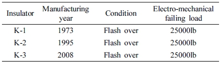
Three aged porcelain insulators, which were manufactured by a same manufacturer and installed in 1973(K-1), 1995 (K-2), and 2008(K-3), and which were removed from the transmission lines, were used. The information on the aged porcelain insulators is shown in Table 1. The internal defects or pores in the three aged insulators were investigated by X-ray 3D CT(Smart CT, Techvalley) and analysed using software(VGStudio MAX 3.0, Volume Graphics). The aged insulators whose microstructures were observed using X-ray 3D CT, were cut to pieces of size 20 mm × 30 mm with thickness of 4 mm, and the microstructures were observed using OM(HRM-300, Huvitz) and FE-SEM(Su-70, Hitachi). The results were compared to those of the X-ray CT. The element compositions of the aged porcelain insulators were obtained by energy-dispersive X-ray spectroscopy(EDS, Oxford). Qualitative and qu- antitative phase analyses were carried out using XRD(D8-Advance, Bruker) analyses to study the phases of the aged insulators. The quantitative phase analyses were carried out by Rietveld refinement method using TOPAS software. Vickers hardness tester(Durascan 70, Emco-test) was used to measure the hardness values of the aged insulators. The load and the dwell time were 5 kgf and 15 s, respectively, and ten indentations were made on the polished surface of each aged insulator.
3. Results and Discussion
Fig. 1 shows the appearance of the cross section of the aged porcelain insulator. The porcelain insulator is composed of a metal cap, porcelain, cement, and steel pin. Fig. 2(a)-(b) show the X-ray 2D CT images of the whole and the half-cut aged porcelain insulator(K-1), respectively. For the whole insulator, the images of the defects were not clearly seen compared to those of halfcut insulator. It is relatively more difficult for the X-ray to pass the metal cap portion of the the insulator than the porcelain part(more X-ray can be absorbed in the metal part than in the porcelain part of the insulator). And so the insulators which were cut by half through the cap and pin were used for the X-ray CT to reduce the X-ray transmission loss by the metal cap and to obtain a large amount of transmitted X-ray in detector, which can lead to CT images of better spatial resolution.
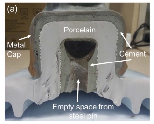
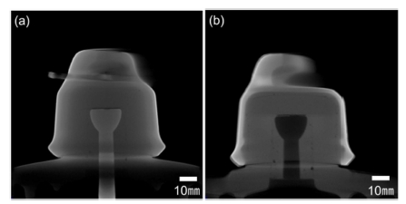
Fig. 3(a)-(c) and Fig. 4(a)-(c) show the X-ray 2D & 3D CT images of the half-cut aged porcelain insulators. Defects with sizes of mm were observed in all samples, and most of the observed defects were found in the cement and near the porcelain/cement interface. The defects which are smaller than mm in size were not detected by X-ray CT, and it was difficult to find any significant correlation between the time in the field and the number/size of defects. In order to compare the images obtained from X-ray CT and OM/SEM, small samples of the three aged insulators which have smooth surfaces were prepared for OM/SEM analyses.
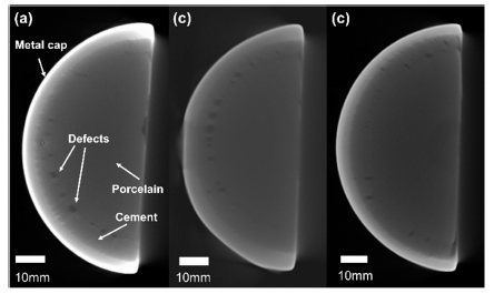
Fig. 3
X-ray 2D CT images of the half-cut aged porcelain insulators (a) K-1, (b) K-2, and (c) K-3. Defects are distributed at the cement and near porcelain/cement interface.
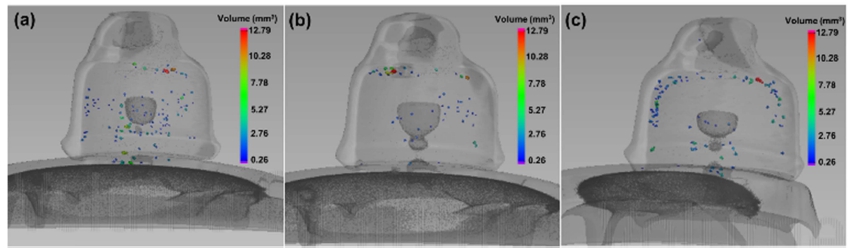
Fig. 4
X-ray 3D CT images of the half-cut aged porcelain insulators (a) K-1, (b) K-2, and (c) K-3. Defects are distributed near porcelain/ cement interface.
Fig. 5(a)-(e) show the appearance and OM images of the small K-1 specimen. The porcelain has dense microstructure, and defects were not observed in the porcelain part of the insulator. Pores were observed at the cement and near the porcelain/cement interface, which is consistent with the result of CT. In addition, the defects with size of um were also observed which were not observed by Xray CT. The OM has better resolution, but it can observe microstructure of a small area compared to X-ray CT. On the other hand, the CT has the disadvan- tage of relatively low resolution, but it has the advantage of being able to observe microstructural features in the whole insulator. The combination of OM and CT can be used for effective analyses of the defects in insulator. Dark and bright parts are observed in the cement part of the insulator [Fig. 5(c)]. From the EDS analyses(the results are not shown), it was confirmed that Si and Ca are the main components in the bright grains, and the dark parts include Al as well as Si and Ca.
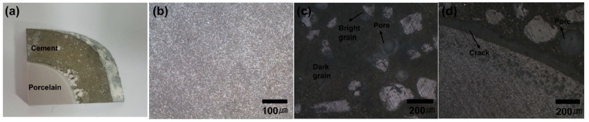
Fig. 5
(a) Appearance and the OM images of the (b) porcelain, (c) cement, and (d) porcelain/cement interface of K-1 insulator.
Fig. 6 shows the microstructure of the porcelain part of the aged insulators K-1 obtained by FE-SEM. The porcelain parts consist of three different regions: dark, bright, and needle-shape grains. It is well known that porcelain part mainly consists of SiO2 and Al2O3. To compare the microstructure and the element composition of three insulators, EDS analyses were carried out, and the results are shown in Fig. 7(a)-(c).
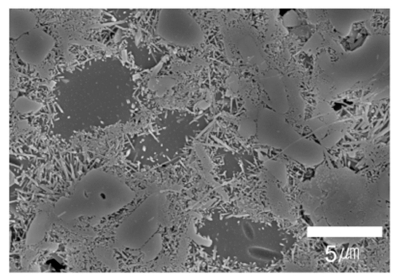
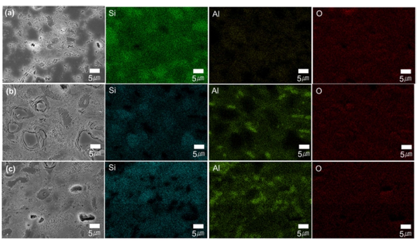
Fig. 7
FE-SEM and EDS images of porcelain part of (a) K-1(1973), (b) K-2(1995), and (c) K-3(2008) insulators. Those with (Si), (Al), and (O) show the distribution of the elements silicon, aluminum and oxygen, respectively.
All samples have three different regions, and it is shown that the dark region has more Si than Al, the bright region has more Al than Si and the needle-shape particles have both Si and Al. The K-1 has large amounts of Si, and K-3 has large amounts of Al, which shows that the insulators which were manufactured more recently have larger amount of Al and smaller amount of Si than those manufactured earlier, which was consistent with what has been reported before.
To understand the differences in microstructure of the aged porcelain insulators(K-1, K-2, and K-3), the qualitative and quantitative XRD phase analyses were performed, and the results are shown in Fig. 8 and Table 2, respectively.
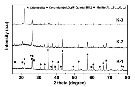
Table 2
Results of X-ray diffraction quantitative analyses of the aged porcelain insulators K-1(1973), K-2(1995), and K-3(2008).
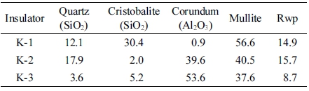 |
All the samples include cristobalite(SiO2, PDF 04- 013-9484), quartz(SiO2, PDF 00-005-0490), corundum (Al2O3, PDF 01-083-2080) and mullite(Al2.22Si0.78O4.89, PDF 01-079-1456), which have been used to manufacture porcelain part of the insulators. The K-1 has large amount of SiO2 and Al2O3. On the other hand, K-2 and K-3 has more Al2O3 contents than K-1. The amounts of SiO2 and Al2O3 are determined by the composition of the starting materials in the manufacturing process.
Carbajal et al.21) reported that for the porcelain insulators produced before the 1980s, SiO2 was mainly used as the raw material. But since 1980, porcelain insulators have been manufactured using Al2O3 instead of SiO2 to improve the electrical and mechanical properties during aging.
That explains the large amount of SiO2 in K-1 which was manufactured in 1973 and large amount of Al2O3 in K-2(1995) and K-3(2008).
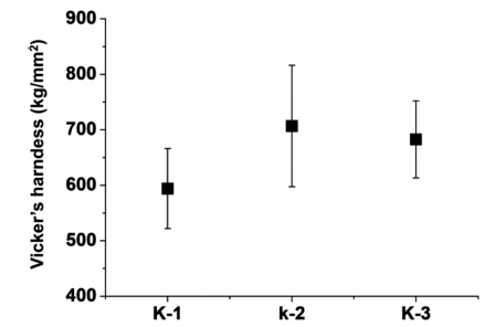
Fig. 9 shows the Vickers hardness of the aged porcelain insulators(K-1, K-2, and K-3). The Vickers hardness of K-2 and K-3 were similar, but that of K-1 was much lower than those of K-2 and K-3. The large amounts of cristobalite(SiO2) in K-1, which can come from the phase transformation of quartz which can result from the manufacturing process, can be responsible for the low hardness.19,22) The difference in the thermal expansion coefficient between quartz and cristobalite can cause stress in the insulator due to volume changes during the heating or cooling processes, which can reduce the mechanical strength of the porcelain insulators.23) As a result, insulators with a large amount of SiO2 are more likely to experience electrical and mechanical failure, compared to insulators with large amount of Al2O3.
4. Conclusion
The microstructure, phase, and mechanical properties of three aged porcelain insulators, which were manufactured in 1973, 1995, and 2008 and which were used in the field for different amounts of time were investigated. The microstructures of the aged insulators were observed by X-ray 3D computed tomography(CT), optical microscopy (OM) and scanning electron microscopy(SEM). The internal defects with sizes of mm are observed at cement and near porcelain/cement interface by X-ray CT. On the other hand, the defects with sizes of um are observed by OM and SEM. The number and size of defects in all the aged insulators were similar. These defects may be caused by the manufacturing process or mechanical stress during use. However, since there is no information on the size/number of defects before the use of these aged insulators, it is difficult to find the origin of defects in this study.
Using qualitative and quantitative phase analyses by XRD, it is found that the insulator which was manufactured in more recent years contain larger amount of Al2O3 and smaller amount of SiO2 than those manufactured earlier. The aged insulator with large amount of SiO2 has lower hardness than those with large amount of Al2O3. The difference in the thermal expansion coefficient between quartz(SiO2) and cristobalite(SiO2) can cause stress in the insulator during an abrupt temperature in the field, which can reduce the mechanical strength of the porcelain insulators.
