

1. Introduction
Piezoelectric materials, known for their ability to interconvert electrical and mechanical energy, are widely utilized in various electronic devices such as sensors, actuators, and energy harvesters.1,2,3,4) Among them, Pb(Zr,Ti)O3-based materials are the most extensively used due to their superior piezoelectric properties. However, the toxicity associated with lead-containing materials has driven the development of lead-free piezoelectric materials.5,4,3,8) Potassium sodium niobate [(K,Na)NbO3]-based ceramics are among the most actively researched lead-free piezoelectric materials. Over the past decade, numerous compositional engineering studies have reported piezoelectric properties comparable to those of Pb(Zr,Ti)O3-based materials.9,10,11,12,13) Furthermore, recent studies have demonstrated the excellent performance of sensors, transducers, and actuators incorporating (K,Na)NbO3-based materials.14,15,16,17)
Research on piezoelectric thin-film materials is also actively progressing for applications in microelectromechanical systems (MEMS), flexible piezoelectric energy harvesters, and piezoelectric nanogenerators.18,19,20) While Pb(Zr,Ti)O3-based materials have been predominantly used in piezoelectric thin-film studies,18,19) research on lead-free (K,Na)NbO3-based thin films has also been reported.20) Various deposition methods, including RF sputtering,21) pulsed laser deposition (PLD),22,23) and the sol-gel method,24) have been employed to fabricate (K,Na)NbO3-based thin films. Among these, studies utilizing sputtering and PLD, representative physical vapor deposition (PVD) methods, have frequently reported issues such as compositional changes due to the high volatility of alkali elements, leading to degradation in piezoelectric performance.23,25,26)
Volatilization of alkali elements during the high-temperature manufacturing process of (K,Na)NbO3-based bulk ceramics has been widely reported.27,28,29) In these bulk ceramic studies, it is often mentioned that sodium volatilizes more readily than potassium.29) Thin film deposition via PVD processes occurs through the consumption of the ceramic target, and studies have been conducted using ceramic targets with excess alkali elements to address the deficiency of alkali elements in (K,Na)NbO3-based thin films.30) To control the composition of thin films, it is important not only to regulate the alkali element content in (K,Na)NbO3-based ceramic targets fabricated at high temperatures but also to monitor the surface compositional changes of the ceramic targets during the deposition process.
This study reports on the effects of alkali element volatilization during the RF sputtering thin-film deposition process on the phase formation, dielectric properties, and ferroelectric properties of (K,Na)NbO3 thin films. In particular, it discusses the volatilization of alkali elements at the ceramic target surface, a phenomenon that has rarely been reported previously. The degree of alkali element volatilization varies with the RF power, both at the surface of the ceramic target and in the deposited thin film. The study highlights that specific RF power and substrate temperature conditions are required to achieve stable perovskite phase formation. Furthermore, unlike in bulk ceramics, it is observed that during thin-film deposition via RF sputtering, the volatilization of the heavier potassium is more pronounced than that of sodium in both the ceramic target and the thin film.
2. Experimental Procedure
The ceramic targets with nominal compositions K0.5Na0.5NbO3 and K0.55Na0.55NbO3 were prepared using a solid-state synthesis method with raw powders of K2CO3 (99 %, Kojundo Korea Co.), Na2CO3 (99.95 %, Kojundo Korea Co.), and Nb2O5 (99.9 %, Kojundo Korea Co.). The raw powders were weighed according to the cation molar amounts and mixed in a nylon container with anhydrous ethanol (99.9 %, Samchun Pure Chemical Co.) and zirconia balls [yttria-stabilized zirconia (YSZ), SciLab]. The mixture was subjected to a primary grinding and mixing process for 24 h using a ball mill. The resulting slurry was dried at 80 °C, and the dried powders were calcined at 825 °C for 6 h (for K0.5Na0.5NbO3) and at 500 °C for 6 h (for K0.55Na0.55NbO3). After calcination, each powder was re-grinded for 24 h using the same ball milling process. The ground powders were then pressed into disk-shaped green bodies with a diameter of 70 mm under 100 MPa pressure. The green bodies were subjected to cold isostatic pressing under 200 MPa pressure for 3 min. Following this, the powder compacts were sintered at 1,100 °C for 50 h (for K0.5Na0.5NbO3) and at 800 °C for 30 h (for K0.55Na0.55NbO3). To suppress alkali element volatilization during the high-temperature sintering process, the powders were muffled in a base powder. The sintered ceramic targets were then processed into disks with a diameter of 50.8 mm and a thickness of 5 mm.
The KNN thin films, deposited using a K0.55Na0.55NbO3 ceramic target, were formed on Pt(111)/Ti/SiO2/Si(100) substrates via the RF magnetron sputtering method (KVS-4000L, Korea VAC). During deposition, the base pressure was maintained below 5 × 10⁻⁷ Torr, and the working pressure was controlled at 10-2 Torr. A gas mixture of Ar and O2 was used as the plasma gas, with a partial pressure ratio of 4 : 1. During deposition, the substrate temperature was maintained at 500~700 °C, and the RF power was adjusted to 20~100 W for thin film deposition. No post-deposition annealing was performed after the thin film deposition. To measure the dielectric and ferroelectric properties of the deposited thin films, circular platinum electrodes with a diameter of 300 µm were deposited on the top surface of the films using an E-beam evaporator (KVE-E2000, Korea VAC).
The structural analysis of the fabricated ceramic targets and deposited KNN thin films was performed using X-ray diffraction (XRD, SmartLab, Rigaku), X-ray photoelectron spectroscopy (XPS, VersaProbe 3, ULVAC-PHI), and field emission scanning electron microscopy (FE-SEM, MIRA3, TESCAN). The elemental composition analysis of the ceramic targets and thin films was carried out using energy-dispersive X-ray spectroscopy (EDX, Xflash 630mini, Bruker). The dielectric constant and dielectric loss of the thin films were measured using an impedance analyzer (E4990A, Keysight), while the polarization versus electric field (P-E) hysteresis curves were obtained using a ferroelectric analyzer (TF3000, aixACCT).
3. Results and Discussion
Fig. 1(a) shows the relative elemental contents normalized to the niobium content of the as-sintered K0.5Na0.5NbO3 and K0.55Na0.55NbO3 ceramic targets. The values indicated by the dashed lines represent the relative elemental contents of the intended stoichiometric K0.5Na0.5NbO3 composition. It can be observed that the alkali element content in the K0.5Na0.5NbO3 ceramic target is deficient compared to the intended composition, suggesting that volatilization of alkali elements occurred during the sintering process. In the case of the K0.55Na0.55NbO3 ceramic target, although some volatilization of alkali elements occurred, it maintained a higher alkali element content than the stoichiometric K0.5Na0.5NbO3 composition. The oxygen content in both ceramic targets was lower than the intended level, with a more significant deficiency observed in the K0.5Na0.5NbO3 ceramic target. Fig. 1(b) presents the XRD pattern and surface SEM image of the as-sintered K0.55Na0.55NbO3 ceramic target, demonstrating that the perovskite structure was well-formed without any secondary phases despite the excess alkali element content. Therefore, in this study, thin films (hereafter referred to as KNN thin films) were deposited using the K0.55Na0.55NbO3 ceramic target, which maintained alkali element content not deficient compared to the intended stoichiometric K0.5Na0.5NbO3 composition.
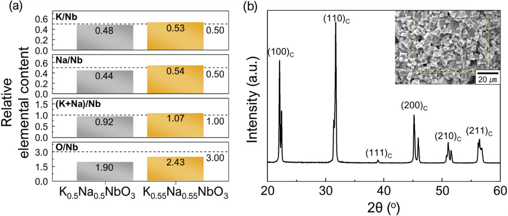
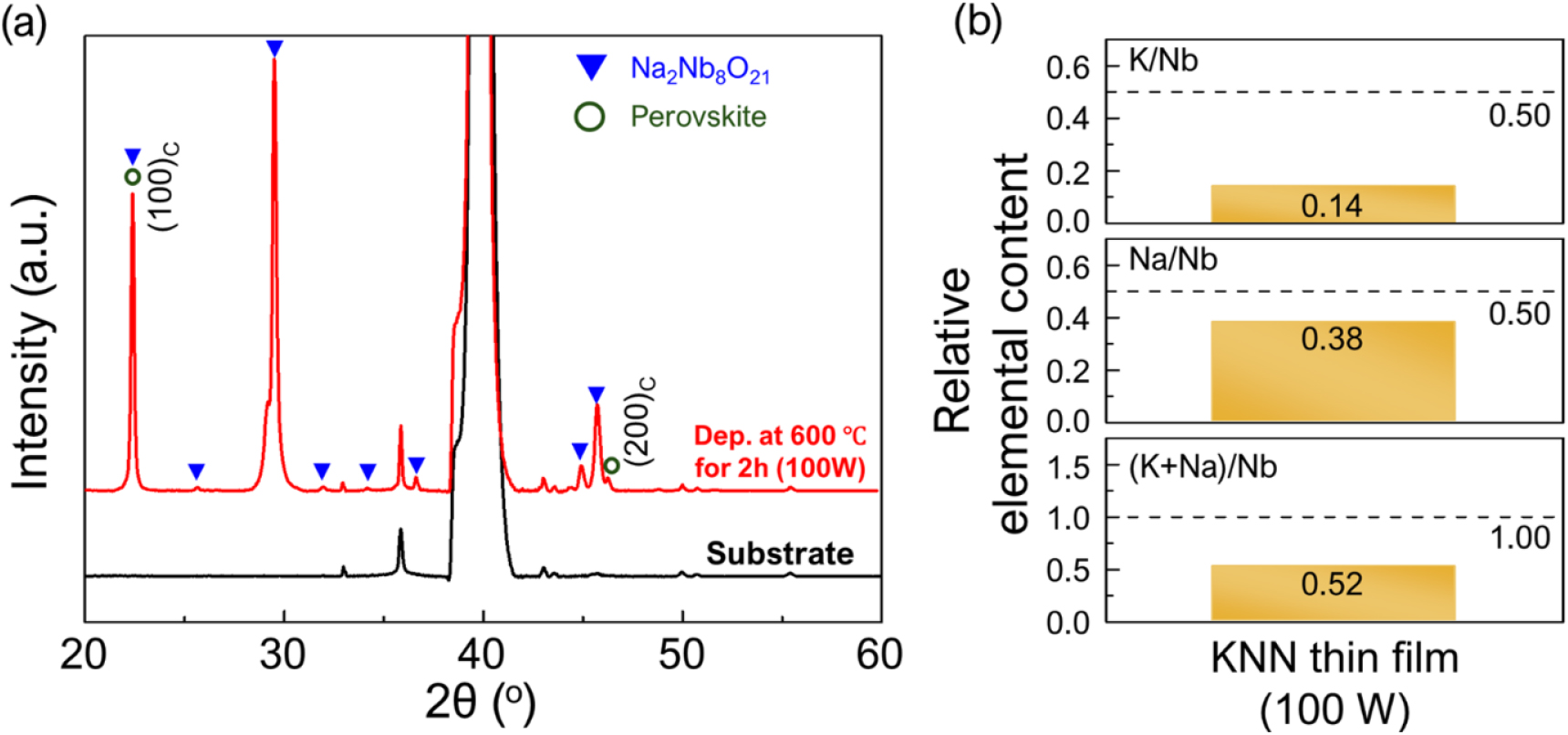
Fig. 2(a) shows the XRD pattern of the KNN thin film deposited for 2 h under the conditions of 100 W RF power and a substrate temperature of 600 °C. Although perovskite (100) and (200) peaks were observed, most of the diffraction peaks were indexed to the Na2Nb8O21 phase. As shown in Fig. 2(b), the alkali element content in the thin film was found to be significantly lower than that of the stoichiometric K0.5Na0.5NbO3 composition, with the potassium content being much lower than the sodium content. Consequently, it is inferred that severe volatilization of potassium occurred during the deposition of the KNN thin film, leading to the formation of the Nb-rich Na2Nb8O21 phase in the thin film.
To further investigate the cause of the severe alkali element deficiency in KNN thin films, the effect of the sputtering process at 100 W RF power on the surface of the K0.55Na0.55NbO3 ceramic target was analyzed. Fig. 3 shows the structural characteristics of the ceramic target surface before and after a single sputtering process conducted at 100 W RF power for 2 h. As seen in Fig. 3(a), the alkali and oxygen contents on the target surface decreased after the sputtering process compared to their levels before sputtering. Nevertheless, the ceramic target retained the perovskite phase, as shown in Fig. 3(b). Additionally, after the sputtering process, the XPS O1s spectrum of the target surface exhibited a noticeable increase in the peak associated with oxygen vacancies (OV, ~531.5 eV), in addition to the peak originating from the oxygen in the normal KNN lattice (OL, ~530 eV) [Fig. 3(c)].
These observations indicate that the volatilization of alkali elements and oxygen occurred on the target surface during the 100 W sputtering process. Interestingly, it was observed that potassium volatilized more readily than sodium, not only in the thin film [as shown in Fig. 2(b)] but also on the ceramic target surface. This suggests that when the KNN ceramic is exposed to RF sputtering plasma, potassium is significantly more volatile than sodium. In particular, under the plasma conditions at 100 W, the lattice stability of potassium is extremely low in both the ceramic target and the thin films deposited at 600 °C. Fig. 3(d) presents the XPS K2p peaks of the ceramic target surface before and after sputtering. Before sputtering, the intensity of the K2p1/2 (~291.8 eV) and K2p3/2 (~294.6 eV) peak pair was high; however, after sputtering, this peak pair nearly disappeared, and the intensity of the satellite peak pair, K'2p1/2 (~293.3 eV) and K'2p3/2 (~296.2 eV), which shifted to a higher energy range, significantly increased. Furthermore, as shown in Fig. 3(b), no traces of secondary phases or amorphous phases were detected on the target surface after sputtering. Considering all the results from Fig. 3, it can be inferred that the K2p1/2 and K2p3/2 peaks originate from potassium atoms in the normal KNN lattice, while the K'2p1/2 and K'2p3/2 peaks are associated with potassium atoms in KNN lattices with high concentrations of vacancies.
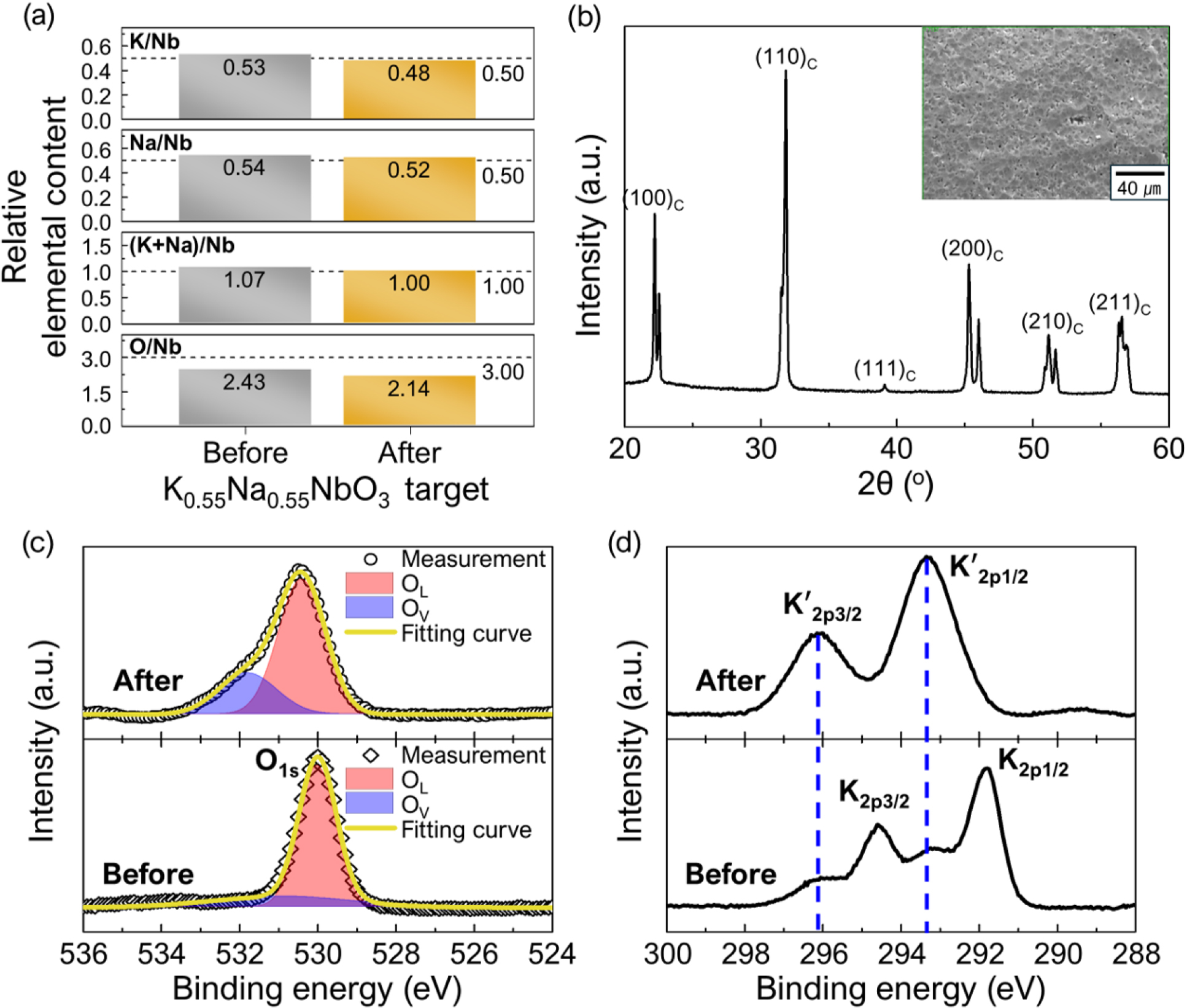
Fig. 3.
Structural characteristics of the K0.55N0.55NbO3 ceramic target surface before and after a single sputtering process conducted at 100 W RF power for 2 h: (a) relative elemental contents, (b) XRD pattern (after sputtering; inset: surface SEM image), (c) XPS spectra for O1s, and (d) XPS spectra for K2p signals.
The RF power of 100 W was not suitable for forming a single-phase perovskite KNN thin film. Therefore, as shown in Fig. 4(a), the sputtering process was conducted at reduced RF powers of 50 W and 20 W. Under the conditions of 50 W RF power and a substrate temperature of 600 °C, a {100}-oriented perovskite phase was well-formed without any secondary phases. However, at 20 W RF power, no crystalline phases were observed. Even after the seventh deposition at the 50 W condition, only the {100}-oriented perovskite phase was observed without the formation of any secondary phases, indicating that 50 W RF power is a suitable condition for reproducibly depositing perovskite KNN thin films without causing elemental volatilization damage to the ceramic target. Fig. 4(b) shows the XRD patterns of KNN thin films deposited at 50 W RF power under different substrate temperatures. When the substrate temperature was lowered to 500 °C, no crystalline phases were observed, suggesting that the thermal energy was insufficient to form the KNN perovskite phase. At a substrate temperature of 700 °C, both {100} perovskite peaks and secondary phase peaks corresponding to Na2Nb8O21 were observed, implying that the high thermal energy during deposition caused active volatilization of potassium elements in the thin film.
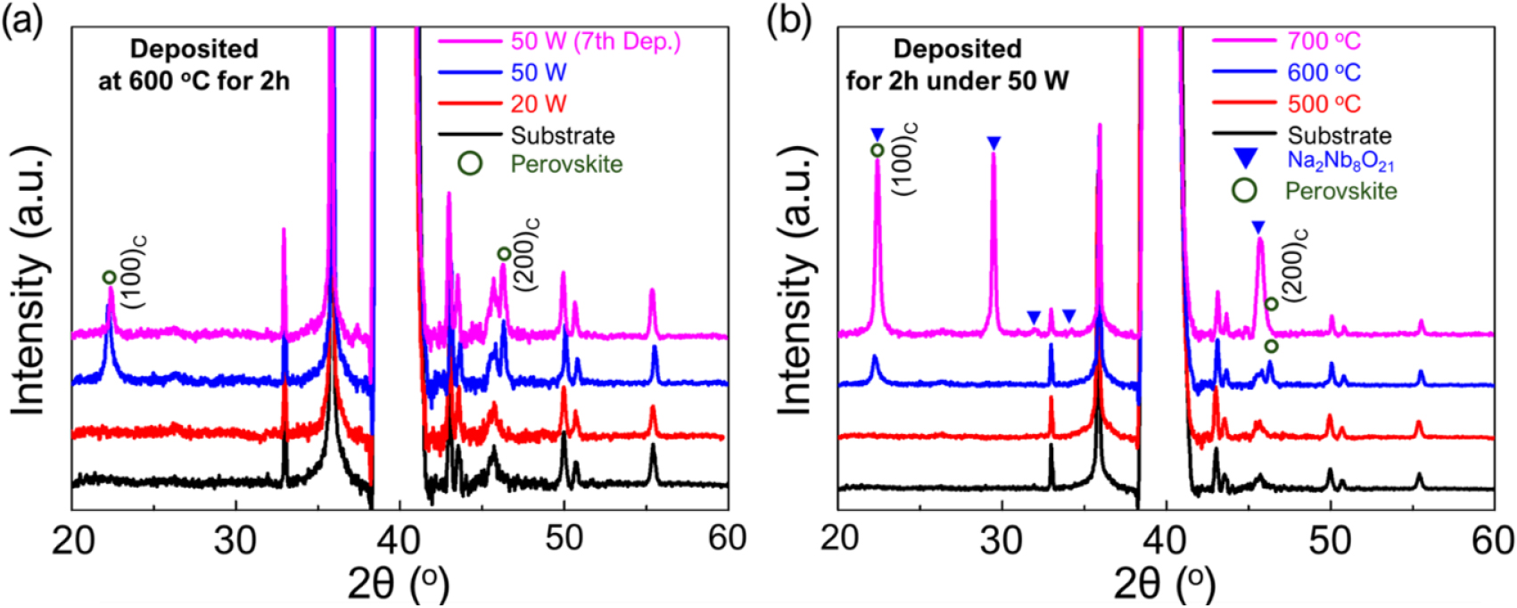
Fig. 5 shows the dielectric and ferroelectric properties of KNN thin films deposited at 50 W RF power and a substrate temperature of 600 °C as a function of film thickness. KNN thin films with thicknesses of 70 nm, 335 nm, and 500 nm were prepared [Fig. 5(a-c)]. Overall, the thin films were deposited with uniform thickness, and no interface defects such as cracks or buckling were observed. As shown in Fig. 5(d), the dielectric constant at 1 kHz increased significantly from 113 for the 70 nm-thick film to 185 for the 335 nm-thick film and slightly further to 195 for the 500 nm-thick film. The sharp decrease in the dielectric constant observed for ultrathin films (on the order of tens of nanometers) is likely due to the effect of the dead layer formed at the interface between the dielectric material and the metal electrodes.31,32,33) Across the frequency range of 1 kHz to 100 kHz, the variation in dielectric constant for all films was less than 5 %, and the dielectric loss variation was below 2.5 %, indicating stable dielectric properties with respect to frequency.
As shown in Fig. 5(e), the maximum polarization value of the 70 nm-thick film, which had the lowest dielectric constant, was the smallest among the films. The slope trends of the P-E hysteresis curves were consistent with the trends in dielectric constant. However, the remnant polarization values of the films were relatively low, ranging from 1.5 to 2.1 µC/cm2, and the P-E hysteresis curves exhibited a slim shape characteristic of relaxor ferroelectrics rather than typical ferroelectrics. According to the EDX analysis of the KNN thin film deposited at 50 W and 600 °C, as shown in Fig. 5(f), potassium content was significantly lower than sodium content, resulting in a sodium-rich solid solution compared to the intended K0.5Na0.5NbO3 composition. This indicates that potassium volatilization still occurred during deposition at a substrate temperature of 600 °C. It appears that a sodium-rich solid solution with a ratio of 0.75 : 0.25 between antiferroelectric NaNbO3 and normal ferroelectric KNbO3 was formed, resulting in relaxor ferroelectric thin films.34,35,36) The dielectric constant of these thin films was also significantly lower than that of K0.5Na0.5NbO3 ceramics with a morphotropic phase boundary (MPB) composition (~450), further supporting this interpretation.37,38)
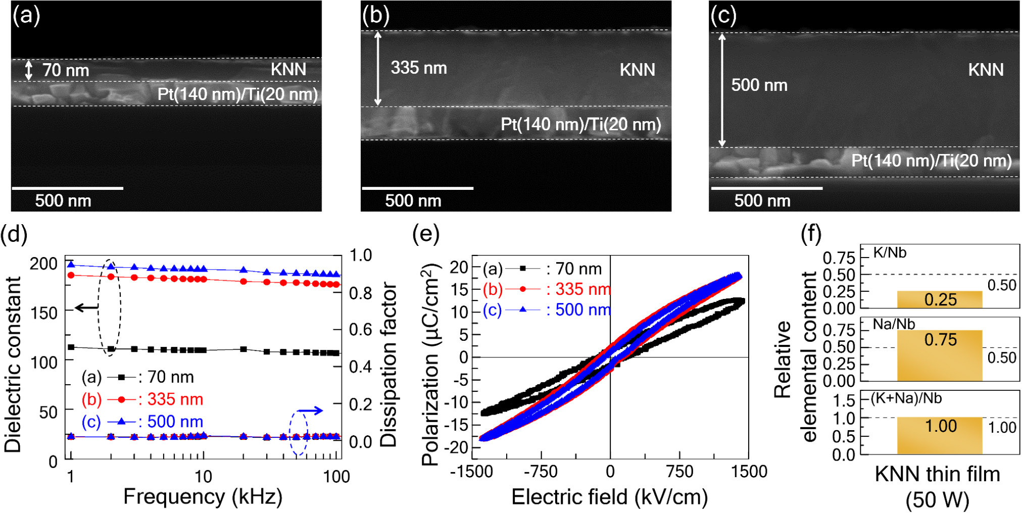
Fig. 5.
(a-c) Cross-sectional SEM images, (d) dielectric constant and dissipation factor spectra, and (e) polarization vs. electric field curves of KNN thin films with various thicknesses deposited under the condition of 600 °C substrate temperature and 50 W RF power. (f) Relative elemental contents of the 335 nm-thick KNN thin film.
4. Conclusion
In this study, the effects of alkali element volatilization occurring on the surface of KNN ceramic targets and in the deposited thin films during the RF sputtering deposition process of KNN thin films were investigated. It was revealed that 100 W RF power accelerates the volatilization of alkali elements (predominantly potassium) from the surface of the KNN ceramic target, significantly compromising the reproducibility of KNN thin film fabrication. A power of 50 W was found to be suitable for reproducibly depositing {100}-oriented perovskite thin films at a substrate temperature of 600 °C. However, in this case, the resulting thin films were relaxor ferroelectric films, with a significant deficiency of potassium compared to sodium. No crystalline thin films were obtained under RF power lower than 50 W or at substrate temperatures lower than 600 °C. Additionally, substrate temperatures higher than 600 °C were found to promote the volatilization of potassium in the deposited thin films. Therefore, maintaining high substrate temperatures during RF sputtering makes it very challenging to replicate the stoichiometry of the ceramic target in the thin films due to potassium volatilization. It is suggested that using a potassium-rich KNN ceramic target may be more suitable for fabricating MPB KNN thin films close to the K0.5Na0.5NbO3 composition.
