

1. Introduction
Integrated circuits(ICs), which are fabricated on large scale semiconductor substrates, require connections between multi-layers of metal to electrically interconnect the discrete layers of semiconductor devices on chips. The different levels of connections are separated by etching through holes of insulating or dielectric layers to be connected on metal layers.
Due to the increasing density of transistors and shrinking sizes of features, the main factors which affect the circuit speed of high quality performance ICs have been recently focused on parasitic capacitance with backend- of line aluminum interconnections and electrical resistance.1-2) By controlling the thickness of insulating layers between interconnections, the inter-level and intralevel capacitance in the metal lines would increase due to the capacitance, which is proportional to the spacing between the lines.
It is important to control the resistor-capacitor(RC) time delay, which affects the capacitance of a circuit. By increasing the RC time delay, it also increases the signal propagation time due to decreases of the circuit frequency response, which improves the circuit performance. Thus, it is essential to reduce the RC time constant. Depositing low dielectric constant k insulating material between the metal lines affects the RC time delay which decreases the RC time delay. Using a low dielectric constant layer decreases the power consumption of the device, which prevents cross-talk between different metal layers.
There have been studies regarding the development of low-k materials, organosilicate glass(OSG, SiCO-H) and carbon-doped oxides have been considered as candidates due to their potential applications. The functional groups in the organic compounds showed increased free volume of the films, which drastically decreases the dielectric constant.3-5) Nevertheless, despite the high porosity, low density, and great characteristics of the new functional groups of low-k organic materials, the elastic modulus, hardness, and absence of delamination have not been demonstrated, which are required to improve the thermal and mechanical stabilities. Additionally, if the density of a circuit increases, the gap widths decrease, which makes the gap aspect ratio, defined as the gap height divided by the width, increase further. As a result, the difficulties of filling gaps with a narrower size grow, and issues such as discontinuities and voids will form in the gap-fill or insulating material.
Previously, we developed Aurora2.7-CxHyOz films and investigated the capability of gap-filling. We obtained low-k films, which have superior electrical and mechanical properties, with super filling on inter metal dielectric(IMD) and shallow trench isolation(STI) patterns. In this paper, we investigated the multi-step deposition of low-k films to increase the adhesion between the metal line and low-k films without delaminating. This multistep process, which leads to improved mechanical properties, is proposed and discussed.
2. Experimental Procedure
The gap-filling of low-k films on an IMD pattern was characterized. The low-k films were deposited by plasma enhanced chemical vapor deposition(PECVD). A main precursor and a different additive were used in this experiment. The main precursor is dimethyldimethoxysilane( DMDMOS), (CH3)2Si(OCH3)2, and the additive is CxHyOz. The film thickness and refractive index of the deposited films were measured by a reflectometer(Nanometrics, 8300XSE) and ellipsometer(Woollam; Spectroscopic Ellipsometers M-2000DI). For electrical characterization, the relative permittivity, leakage current density, and breakdown field strength were measured at 1 MHz with a solid state measurements(SSM) Hg probe system. The errors of the capacitance and the mercury electrode area were less than 1 %. The trench filling properties were determined by scanning electron microscopy(SEM).
3. Results and Discussion
The principle of gap-fill PECVD is presented in Fig. 1, showing the main precursor and additive compositions for deposition on the trench patterns. This deposition process can be divided into three different stages. First, the film grows in a conformal manner and then, secondly, it begins to grow much faster on the trench bottom of the features than on the other parts of the substrates. Third, after the completion of bottom up filling, the film growth rate abruptly slows down to the initial growth rate. As a result, the submicrometer features are filled in a bottom up fashion, and after the completion of the bottom up filling, the surface becomes level.6)
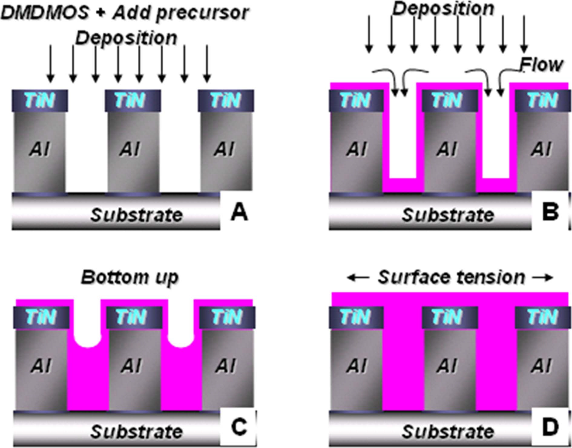
Fig. 1.
Schematic sequence of the trench filling process by bottom up growth of the PECVD process. A. The main precursor and additive composition are deposited on the trench pattern. B. During deposition, the composition flows into the trench pattern. C. The composition can fill perpendicularly upward from the trench bottom, so called “bottom up filling”. D. After the completion of bottom up filling, the film is spread over the patterned metal layer.
However, unlike in the previous image, after the post-thermal annealing treatment, delamination occurred between the metal patterns and low-k films because of shrinkage accompanied by thermal stress. Fig. 2 illustrates the delaminating issue and corresponding SEM images are presented. In order to prevent delamination, multistep deposition consisting of multi plasma treatment and baking treatment was employed.
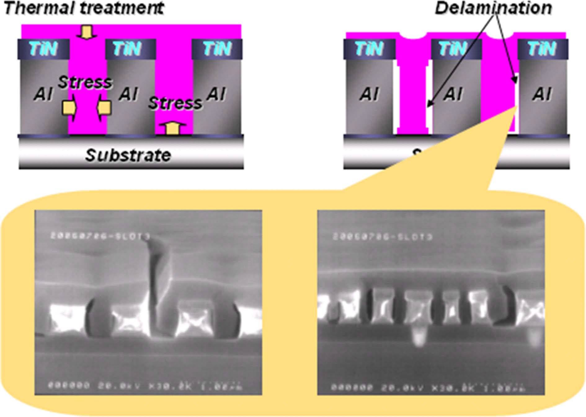
Fig. 2.
Schematic sequence and cross-sectional scanning electron microscopy images after heat treatment.
Fig. 3 shows the schematic sequence of the multi-step deposition process. The pre-treatment (O2 or He plasma treatment) was carried on trench patterns for 30-60 second to improve the adhesion between the deposited low-k films and trench patterns. After the pre-treatment, DMDMOS and the additive precursor were deposited for 30 seconds. Finally, the deposited low-k films were baked at 400 °C for 60 second in the post treatment step. These multi-step processes were carried out for 3-6 cycles to complete the gap-filling without delamination.
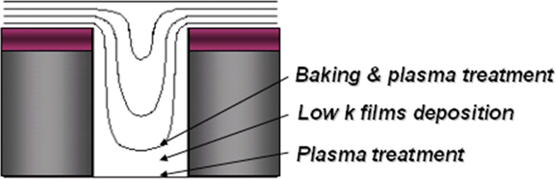
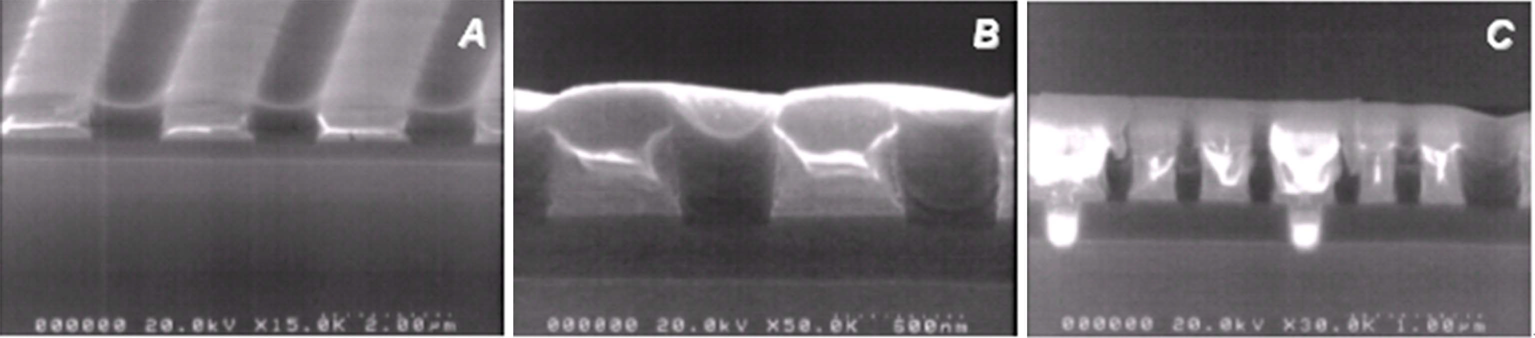
Fig. 4 shows the cross-sectional SEM images of the multi-step deposition process on different trench patterns (1,000 nm-150 nm width, 700 nm depth) after baking for 1 min. Even after a very short deposition time, the deposits showed a transition from being sub-conformal to somewhat conformal at the side wall of the trench. Further, the trench structure is completely filled and the filling sequence of the trench is controlled because a longer deposition time is required to complete the bottom up filling of large trenches rather than small trenches. This represents a very promising result for realizing gapfilling for IMD and STI using the CVD process.
4. Conclusions
A multi-step deposition process for the gap-filling of submicrometer trenches using DMDMOS, (CH3)2Si(OCH3)2, and CxHyOz by plasma enhanced chemical vapor deposition is presented. We obtained low-k films which possess superior gap-filling properties on the trench patterns without voids or delamination. The newly developed technique, which is a multi-step process for gap-filling of submicrometer features, will have a great impact on intermetal dielectrics and shallow trench isolating for next generation microelectronic devices. Moreover, this bottom up gap-fill mode is expected to be universal to other chemical vapor deposition systems.
