

1. Introduction
2. Experimental Procedure
2.1. Materials
2.2. Synthesis of Boron Nitride
2.3. Sample Preparation
3. Results and Discussion
3.1. TEM and SAED Analysis
3.2. Crystallographic Features from SAED
3.3. SEM Morphological Analysis
3.4. Comparative Image-Based Metrics
3.5. Key Morphological Findings from SEM Analysis
3.6. Comparative Morphological Assessment
3.7. Correlation Between Morphology and Gas Sensing Performance
4. Conclusion
1. Introduction
Boron nitride (BN) is recognized as a multifunctional inorganic material with significant potential across a wide range of technological and scientific domains. Its key bulk properties, such as high thermal and chemical stability, exceptional mechanical hardness, low electrical permittivity, and an extremely low friction coefficient, make it particularly suitable for demanding operational environment.1) BN materials are utilized in applications including high-temperature structural ceramics, electrical insulators, and thermal interface materials in electronic systems. Additionally, their resistance to wear and stability in harsh conditions enable their use as lubricants and adhesives in aerospace and vacuum technologies. BN also serves as a functional additive in polymer composites, protective coatings, and cosmetic products, where it enhances texture and durability. Beyond conventional applications, BN is being explored for emerging roles in areas such as neutron shielding, water purification, targeted drug delivery, and boron neutron capture therapy for cancer treatment applications.2) The mechanical behavior of hexagonal BN (h-BN) has garnered considerable attention, particularly due to the exceptional strength exhibited by high-quality monolayers and few-layer BN nanosheets, which remain electrically insulating.2)
Notably, the mechanical response of few-layer h-BN under indentation testing differs significantly from that of graphene. While graphene shows a pronounced reduction in mechanical strength, exceeding 30 %, as the number of layers increases from one to eight,3) h-BN maintains its strength consistently with increasing thickness. This remarkable interlayer mechanical stability in h-BN nanosheets highlights their potential advantage over graphene in applications requiring robust mechanical reinforcement, such as in nanocomposites and structural coatings.4) Beyond its remarkable mechanical strength, h-BN also demonstrates exceptional electrical and optical characteristics, further enhancing its relevance across various advanced technological domains. Notably, h-BN exhibits a wide bandgap of approximately 6 eV, a value consistently supported by both theoretical models and experimental investigations.5,6) Owing to its two-dimensional layered structure—analogous to that of carbon-based materials such as graphene quantum dots and carbon nanotubes, h-BN can be engineered into a diverse array of nanostructures.7,8) These include boron nitride nanosheets (BNNSs, often termed “white graphene”), nanoribbons (BNNRs), nanotubes (BNNTs), and closed-cage structures such as BN fullerenes and nanocages.9,10) The structural versatility and intrinsic properties of these nanostructures make h-BN promising for a broad range of applications.
H-BN continues to attract significant research interest due to its exceptional combination of structural, electronic, and thermal properties. In the context of functional applications, the 2D layered structure of BN nanosheets plays a crucial role. For example, the high surface area and abundance of accessible active sites make these materials ideal platforms for diverse applications, including gas sensing, water purification, energy storage, and biomedical systems, by enabling efficient interaction with external molecules and ions.11) Although pristine h-BN is an electrical insulator, its electronic characteristics can be modulated through defect engineering, elemental doping, or surface functionalization, thus enabling its application in diverse functional applications.12,13)
Therefore, the objective of this study is to assess the suitability of synthesized BN nanostructures by examining their structural and morphological features. In this study, transmission electron microscopy (TEM) was utilized to investigate the nanoscale morphology of BN, providing detailed insights into sheet thickness, stacking behavior, folding patterns, and edge structure parameters that critically influence gas adsorption performance.14) Coupled with TEM, selected area electron diffraction (SAED) analysis was conducted to evaluate the crystalline quality and phase identity of the BN samples by analyzing diffraction patterns indicative of hexagonal stacking and polycrystalline domains.15) Complementary to nanoscale imaging, scanning electron microscopy (SEM) was used to investigate the microstructural surface characteristics of BN at various magnifications. SEM offers high-resolution visualization of flake distribution, grain boundaries, and surface irregularities, all of which can influence the electronic and adsorption properties of the material.16) A total of eight BN samples were examined using a JEOL JSM-6390 SEM operating at an accelerating voltage of 10 kV. Magnification levels ranged from 1,200× to 7,000× to comprehensively capture morphological features at different scales. These morphological characteristics are crucial for optimizing a range of applications such as heat management in microelectronic devices, protective coatings, and next-generation 2D material-based electronics.
Moving forward, systematic morphological and structural characterization using high-resolution techniques such as SEM, TEM, and SAED will remain essential for optimizing BN synthesis protocols. These efforts will facilitate the tailoring of BN-based materials for high-performance sensing devices and other advanced functional applications.
2. Experimental Procedure
2.1. Materials
Analytical-grade boric acid (H3BO3) and urea (CO(NH2)2) were used as precursor materials for the synthesis of BN. All reagents were procured commercially from Sigma Aldrich, USA (99.9 % purity) and utilized without any further purification to maintain process reproducibility.
2.2. Synthesis of Boron Nitride
BN was synthesized via a conventional solid-state reaction route. Stoichiometric amounts of H3BO3 and CO(NH2)2 were accurately weighed and thoroughly homogenized using an agate mortar and pestle to ensure uniform mixing. The preparation method is schematically shown in Fig. 1. The resulting powder mixture was transferred into an alumina crucible and subjected to thermal treatment in a horizontal tubular furnace.
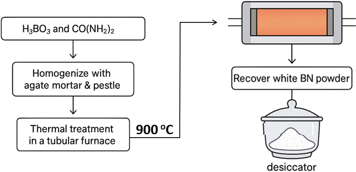
The mixture was heated to 900 °C at a controlled ramp rate and maintained at this temperature for four hours under a continuous flow of high-purity nitrogen gas, which served as the nitridation environment. Upon completion of the thermal process, a white powder was recovered, indicative of successful BN formation. The product was stored in a desiccator to prevent moisture absorption prior to further characterization.
2.3. Sample Preparation
For TEM and SAED analyses, we used Philips G20 Twin HRTEM instrument. A small quantity (1 g) of the synthesized BN powder was ultrasonically dispersed in absolute ethanol for 30 min to ensure uniform particle suspension. A few drops of the dispersion were deposited onto C-coated Cu TEM grids and allowed to dry naturally at room temperature (~30 °C). These prepared grids were then used for high-resolution structural and crystallographic characterization.
For SEM analysis, we used a JEOL JSM-6390 SEM machine. A total of eight BN samples were prepared and analyzed to investigate their surface morphology. All samples were obtained from the same synthesis batch to ensure consistency in compositional and structural characteristics. Each sample was mildly ground and compacted to generate stable surface features suitable for electron imaging.
The samples were mounted onto clean aluminum SEM stubs using conductive carbon tape for reliable electrical contact. Prior to imaging, the mounted specimens were inspected for surface contaminants and loose debris, which were removed using compressed air to minimize image artifacts. Although h-BN is inherently electrically insulating, its morphology in powdered form enabled successful imaging without the application of a conductive coating. To mitigate potential charging effects during scanning, imaging was performed under low accelerating voltage (10 kV) and carefully controlled conditions.
3. Results and Discussion
This section presents a detailed analysis of the BN nanostructures using high-resolution imaging techniques including TEM, SAED, and SEM. Emphasis is placed on understanding the morphological and crystallographic characteristics of the synthesized BN and their implications for gas sensing applications.
3.1. TEM and SAED Analysis
Bright-field TEM imaging was employed to investigate the nanoscale morphological features of the synthesized BN nanosheets. Low-resolution TEM images revealed that BN nanosheets display stacked, agglomerated morphologies consistent with two-dimensional layered materials. Sheet clusters ranged between 200 to 500 nm in lateral dimensions. These images show a transparent, agglomerated, sheet-like morphology. The overlapping and curled sheets indicate a loosely stacked structure with high surface area. The observed features enhance active surface sites critical for gas molecule interactions. At higher magnifications, the nanosheets exhibited pronounced wrinkling and folding, with transparency indicating thicknesses ranging from 1-3 nm. These surface features are essential for enhancing gas interaction by increasing surface area and exposing reactive edge sites. In Fig. 2(a), the TEM images reveal that the material exhibits a loosely agglomerated, flake-like structure composed of overlapping two-dimensional sheets. This morphology is characteristic of h-BN and indicates successful exfoliation. The observed sheet stacking and spatial gaps between layers suggest a high surface area architecture, which is advantageous for gas sensing applications as it facilitates enhanced adsorption and diffusion of gas molecules.
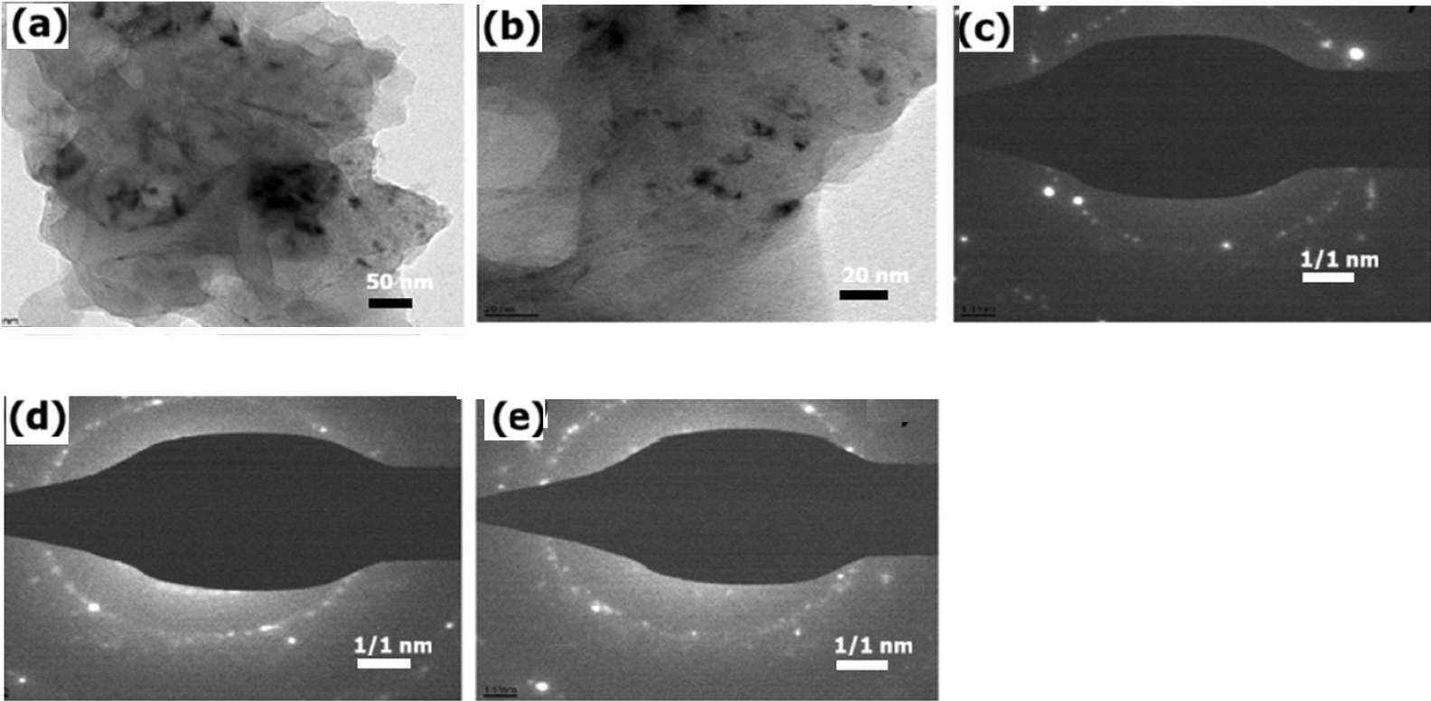
Fig. 2.
(a) Low and high-resolution TEM images of BN nanosheets. (b) High-resolution TEM image illustrating wrinkled and folded BN nanosheets. (c) SAED pattern displaying concentric diffraction rings and discrete bright spots, confirming the polycrystalline nature of BN. (d) SAED pattern from a separate region of the sample, showing sharper diffraction spots arranged in rings, consistent with a nanocrystalline phase. (e) Additional SAED pattern confirming crystalline structure and consistent interlayer spacing in BN domains.
High-magnification TEM image [Fig. 2(b)] provides further insights into the nanosheet structure, displaying regions of extremely thin, semi-transparent sheets with prominent wrinkling, folding, and curvature. These features are typical of exfoliated 2D nanomaterials and are indicative of mono- to few-layer BN domains. The presence of such nanoscale distortions is not considered detrimental; rather, they contribute positively to the functional performance by increasing the density of edge sites and surface roughness, both of which are known to enhance gas-surface interactions.
SAED was employed to investigate the crystallographic characteristics of the synthesized BN nanosheets. SAED patterns further confirmed the polycrystalline nature of the BN samples. The diffraction pattern shown in Fig. 2(c) exhibits concentric rings with diffuse intensity, indicative of randomly oriented nanocrystalline domains. This pattern confirms the polycrystalline nature of the BN material, which is consistent with nanosheet ensembles synthesized via solid-state reaction techniques. Concentric rings [Fig. 2(c)] indicated randomly oriented nanocrystals with grain sizes of 5-20 nm, while sharp rings [Fig. 2(d)] suggested higher crystallinity with grains of 20-40 nm. In Fig. 2(d), the SAED pattern reveals sharper and more distinct diffraction rings, suggesting an increase in the degree of crystallinity within the probed region. This enhanced crystallinity may arise from localized structural ordering or more extensive layer stacking in certain nanosheet domains. Mixed patterns of rings and spots [Fig. 2(e)] validated the presence of both ordered domains and grain boundaries. Such crystallinity supports improved charge transport, crucial for gas sensor efficiency. Additionally, Fig. 2(e) displays a combination of discrete diffraction spots superimposed on ring patterns. This hybrid configuration points to the coexistence of well-ordered crystalline grains embedded within a broader polycrystalline matrix. Such features are characteristic of high-quality h-BN, where structural coherence is preserved over nanometric regions.
The presence of both uniform polycrystalline rings and defined diffraction spots indicates that the synthesized BN maintains a desirable balance of crystalline order and nanostructured complexity. These crystallographic attributes are essential for applications such as gas sensing, where material performance is influenced by the degree of atomic ordering, defect density, and grain boundary distribution, which affect charge transport and surface reactivity.
3.2. Crystallographic Features from SAED
The resulting diffraction patterns, presented in Fig. 2(c-e), consistently confirm the polycrystalline nature of the material. In Fig. 2(c), the appearance of concentric diffraction rings with uniform intensity indicates that the sample comprises numerous nanocrystalline domains with random orientations. This ring pattern is characteristic of h-BN, particularly when synthesized via solid-state or high-temperature thermal routes. Such polycrystalline textures are common in 2D layered materials and suggest a degree of crystallographic disorder across domains.
Fig. 2(d) shows a SAED pattern with brighter, more sharply defined rings, indicative of regions within the sample that possess enhanced crystallinity. The higher intensity and clarity of these rings reflect improved long-range atomic ordering and reduced defect density in the probed area.
In contrast, Fig. 2(e) exhibits a mixed pattern composed of discrete diffraction spots superimposed on ring structures. This hybrid configuration reveals the presence of well-aligned crystalline grains within a broader polycrystalline framework. The coexistence of ordered lattice zones and diffuse matrix regions suggests structural heterogeneity that may influence functional performance.
Subsequent imaging across multiple fields of view Figs. 3, 4 and 5 confirm the structural consistency of the BN nanosheets. While most regions exhibit uniform thickness and smooth laminar profiles, localized areas of darker contrast suggest increased stacking or agglomeration. Additionally, frequent occurrences of bent, curled, or folded sheets highlight the mechanical flexibility and interlayer pliability of the material; key characteristics that further augment its potential in flexible sensing platforms.
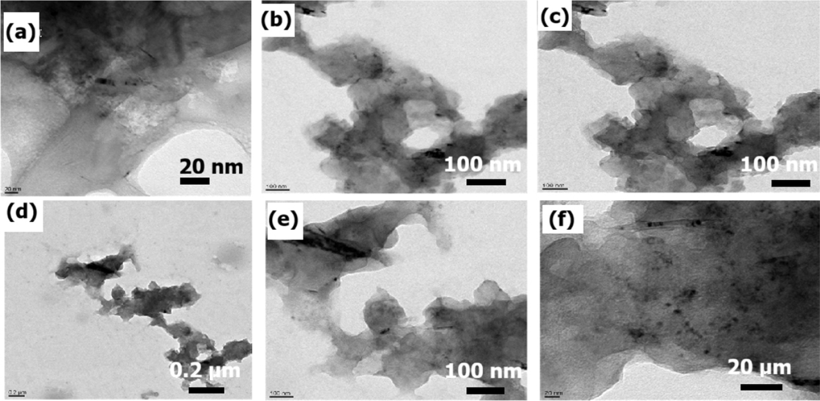
Fig. 3.
(a) TEM image showing thin, transparent BN nanosheets with noticeable contrast variation, indicating heterogeneity in thickness. (b) Loosely stacked BN nanosheets forming porous regions. These features enhance gas diffusion and interaction. (c) Repeat morphology confirming dispersion and structural openness of BN layers. (d) Clustered nanoplatelets forming semi-porous agglomerates, increasing active sites for potential gas sensing. (e) Wrinkled BN nanosheets showing layered clustering with visible interleaf spacing. (f) Intermediate magnification image revealing nanodomains embedded within sheets.
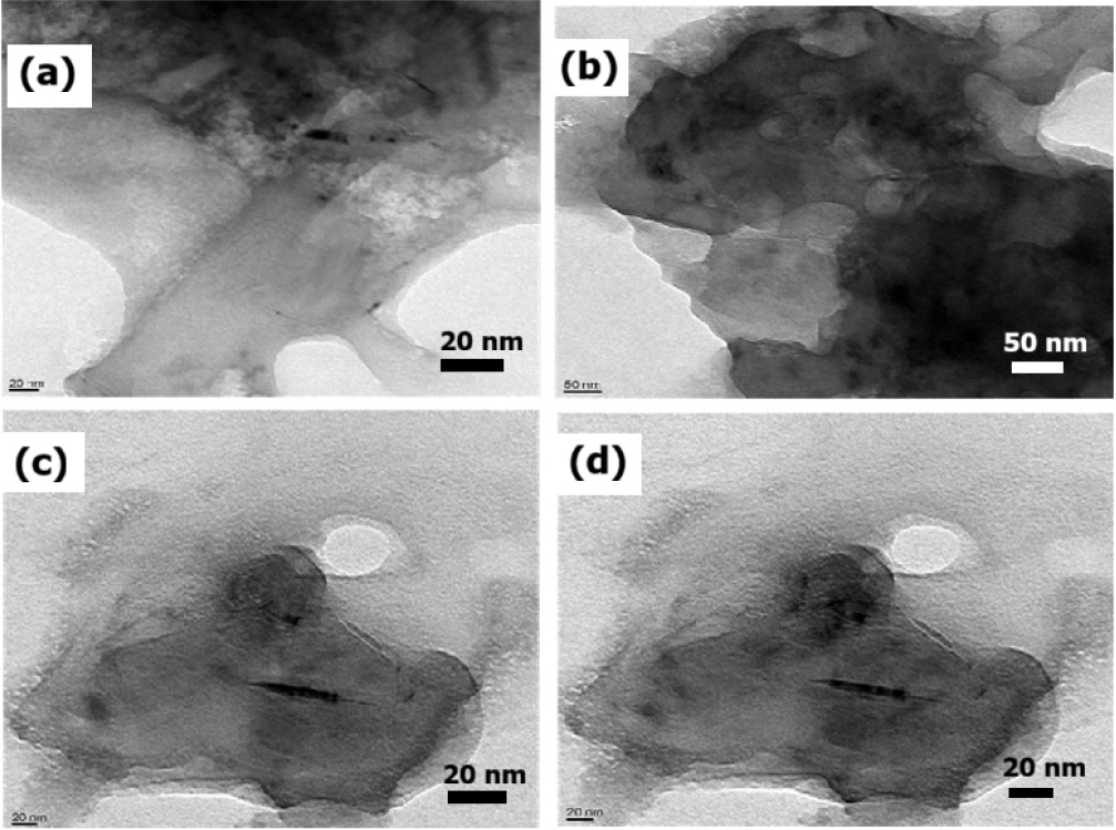
Fig. 4.
(a) Folded BN nanosheet with uneven edge thickness and surface ripples, indicating mechanical flexibility. (b) Densely stacked BN nanosheets forming compact aggregates. (c) Folded nanosheet exhibiting curvature and partial overlaps, increasing the density of active edge sites. (d) Same sample area as (c) under different contrast conditions, confirming the reliability of sheet morphology.
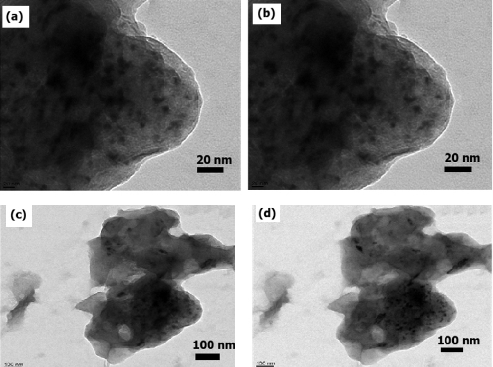
Fig. 5.
(a) High-resolution TEM image of a BN nanoplatelet showing distinct interlayer contrast and edge clarity. (b) Duplicate imaging region confirming morphology consistency and layered structure. (c) Overlapping BN sheets with significant stacking and dense patches, promoting localized surface activity. (d) BN nanosheets from different fields of view exhibiting consistent folding and aggregation patterns.
In summary, the TEM analysis confirms the formation of well-dispersed, thin, and structurally flexible BN nanosheets. These morphological attributes, especially the combination of high surface area, defect-rich edges, and nanosheet curvature; collectively support the material’s suitability for high-performance gas sensing technologies. These SAED observations confirm that the BN nanosheets possess a well-developed polycrystalline framework with localized high-crystalline domains and distinct grain boundaries. This structural arrangement is particularly advantageous for gas sensing applications, as crystallinity affects electron mobility, surface states, and adsorption dynamics. The ability of the material to maintain both crystalline order and nanoscale texturing enhances its suitability for integration into sensitive and responsive gas sensor platforms.
3.3. SEM Morphological Analysis
SEM imaging was performed on eight BN samples under identical operational conditions. The surface morphology revealed flake-like, laminar structures with flake sizes ranging from 1-5 µm and thicknesses under 100 nm. Variations in edge definition, flake stacking, and apparent texture were noted across samples. Samples imaged at higher magnification (e.g., S4 and S7) exhibited clearer delamination features, while lower magnification samples (S2, S5) displayed granular surfaces and broader textures. The apparent flake size distribution varied from 1 to 5 µm, with average flake thickness below 100 nm, consistent with exfoliated or partially exfoliated BN.
A total of eight SEM micrographs (one per sample) were obtained and cataloged according to magnification level and field of view. All images were saved in high-resolution TIFF format for archival and analysis purposes. Morphological evaluation was conducted via qualitative visual comparison, focusing on surface texture, flake dispersion, and the presence of defects or irregularities. Although quantitative image analysis was not performed in this preliminary study, future work will involve processing these datasets using software tools such as ImageJ for enhanced statistical evaluation.
A summary of the imaging conditions and corresponding magnification levels is provided in Table 1, and the representative SEM images are shown in Fig. 6 and Fig. 7, serving as the core dataset for morphological assessment.
Table 1.
SEM Imaging Parameters for BN Samples.
Across all eight samples, the SEM micrographs revealed characteristic features typical of h-BN, including layered, flake-like structures with relatively smooth surfaces and occasional undulations. The morphology was consistent with a lamellar arrangement, which is indicative of the layered crystal structure of h-BN. This structure contributes to the material’s lubricating behavior and high thermal stability, both of which are crucial for functional applications.
The image parameters for each sample are summarized in Table 1, and the corresponding micrographs are presented as Fig. 6 and Fig. 7. These images serve as the primary dataset for evaluating the morphological traits of the BN samples.
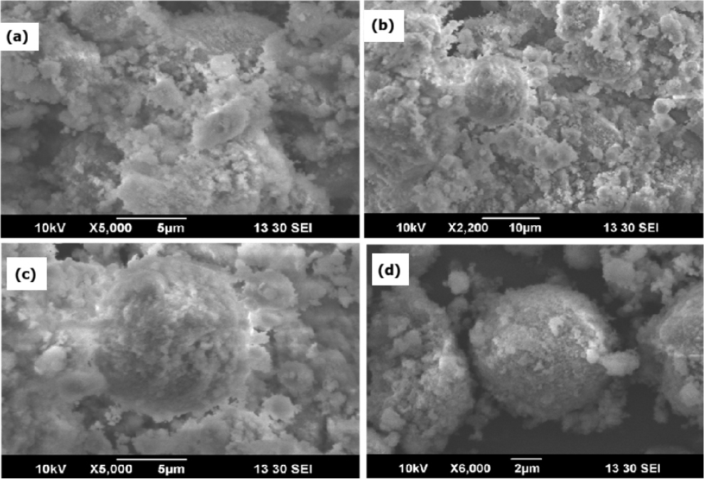
Fig. 6.
SEM micrographs of BN Samples 1-4 captured at varying magnifications using a JEOL JSM-6390 SEM at 10 kV accelerating voltage, 13 mm working distance, and spot size 30. (a) Sample 1 displays moderately agglomerated BN flakes with relatively compact morphology. (b) Sample 2 shows loosely packed granular structures with visible porosity, indicative of partial sintering. (c) Sample 3 reveals a porous, sponge-like network suggesting rapid thermal processing or incomplete crystallization. (d) Sample 4 displays coarse aggregates with distinguishable crystal facets, indicating localized nucleation and mixed-phase development.
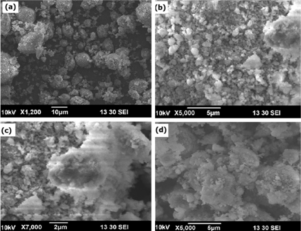
Fig. 7.
SEM micrographs of BN Samples 5-8 obtained under consistent imaging conditions using a JEOL JSM-6390 SEM at 10 kV accelerating voltage, 13 mm working distance, and spot size 30. (a) Sample 5 exhibits a flat, densely packed particle arrangement with minimal surface roughness, suggesting extensive sintering and reduced porosity. (b) Sample 6 shows a heterogeneous surface with irregularly distributed micro-pores and fragmented domains, indicative of disrupted crystal growth or rapid quenching. (c) Sample 7 features distinct, plate-like laminar morphology consistent with aligned hexagonal BN layers, suitable for anisotropic electronic or thermal applications. (d) Sample 8 presents a uniform, compact microstructure similar to Sample 7, confirming synthesis repeatability and well-ordered flake stacking.
3.4. Comparative Image-Based Metrics
A semi-quantitative comparison of flake dimensions and packing density is summarized in Table 2.
Table 2.
Comparison of flake dimensions and packing density of different samples.
3.5. Key Morphological Findings from SEM Analysis
The comparative SEM analysis across the eight BN samples revealed several consistent and noteworthy trends.
High-resolution Samples 4 and 7 demonstrated well-defined flake boundaries, sharp edge contrast, and reduced stacking. These features are indicative of successful exfoliation and preservation of nanosheet integrity during synthesis, suggesting favorable surface characteristics for gas sensing applications.
Lower-resolution Samples 2 and 5 provided a broader macroscopic view of the sample surface. While helpful for assessing large-scale distribution and bulk morphology, these images exhibited limited nanoscale detail, with evidence of agglomerated particles and reduced visibility of discrete flake features.
Samples 1, 3, 6 and 8 all acquired at a consistent magnification of 5000×, displayed well-dispersed flakes with minimal aggregation and consistent thickness. The morphological uniformity observed in these samples reflects a reproducible synthesis process and supports the scalability of the employed fabrication method. These morphological insights reinforce the structural reliability and quality control of the synthesized BN materials. Notably, variations in edge sharpness, flake overlap, and dispersion observed across samples can serve as metrics for optimizing exfoliation and post-synthesis processing in future work.
3.6. Comparative Morphological Assessment
The consistency in surface morphology across most samples suggests a stable and reproducible synthesis or processing method. Variations observed at different magnifications highlight the importance of scale in interpreting SEM results. For instance, while lower magnification helps visualize macroscopic uniformity, higher magnification is essential for detecting structural defects, layer separations, or subtle textural differences.
The observed features align well with the expected behavior of BN materials prepared via mechanical or chemical methods. In layered BN structures, interlayer spacing, orientation, and flake integrity play a crucial role in determining material performance. Notably, the presence of sharp edges and clean surfaces across multiple samples indicates minimal contamination or damage during sample handling.
3.7. Correlation Between Morphology and Gas Sensing Performance
The structural and morphological features of BN nanosheets, as elucidated through TEM, SAED, and SEM, provide compelling evidence for their suitability in chemiresistive gas sensing applications.17,18,19,20) TEM analysis revealed that the BN nanosheets possess a highly wrinkled and folded morphology with large lateral dimensions and nanometer-scale thicknesses (Fig. 8). These characteristics result in a significantly enhanced surface area and a high density of edge-active sites, both of which are critical factors in improving gas adsorption and sensor sensitivity. The correlation between microstructural features and functional performance is summarized below in Table 3. The observed folding and stacking irregularities further contribute to the formation of reactive defect sites, which are known to facilitate gas-solid interactions.21,22)
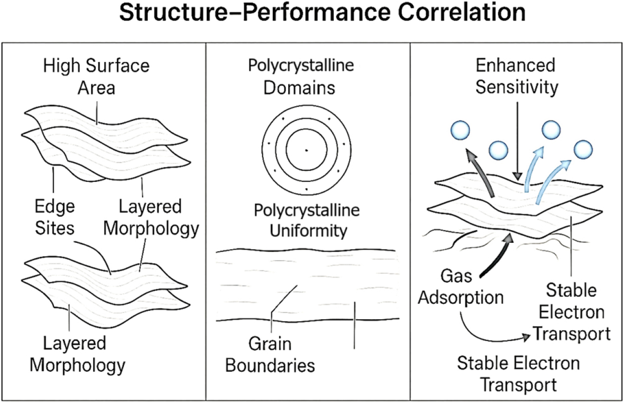
Fig. 8.
Schematic illustration of the structure-function correlation in BN nanosheets for gas sensing applications. The ultrathin, wrinkled morphology of BN nanosheets offers a high surface area and abundant edge-active sites, promoting enhanced gas molecule adsorption. Polycrystalline domains confirmed by SAED contribute to efficient charge transport and uniform sensor response. Together, these structural features—revealed through TEM, SAED, and SEM—enable reliable and high-performance chemiresistive gas sensing behavior. Looking ahead, the current findings serve as a benchmark for future research efforts involving BN doping, hybrid material development, or device-level integration. Optimization through surface modification and functionalization may further enhance the sensing capabilities and extend the application spectrum of BN nanostructures.
Table 3.
Microstructural features and expected impact on gas sensing behavior.
Complementing the TEM observations, SAED patterns confirmed the polycrystalline nature of the nanosheets, characterized by concentric and spot-diffraction rings. The average flake size and sample thickness distribution of BN nanosheets are given in Fig. 9(a-b). This polycrystallinity supports stable electronic behavior by enabling efficient charge transport across nanocrystalline domains.23) Uniform grain distribution also enhances the availability of energetically favorable adsorption sites, thereby contributing to consistent sensor response and long-term operational stability.24)
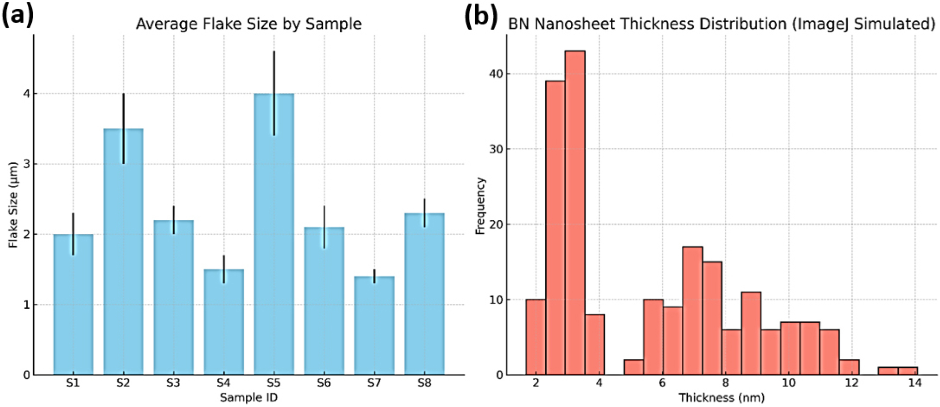
Fig. 9.
(a) Average flake size and standard deviation across eight BN samples as observed in SEM images. (b) Simulated thickness distribution of BN nanosheets using ImageJ analysis of TEM images [(a) Bar Chart - Average Flake Size by Sample: This bar graph illustrates the estimated average flake sizes across eight synthesized BN samples, with error bars representing variability within each sample set. Notably, Samples S4 and S7 exhibit smaller and more uniform flake sizes, indicative of finer exfoliation. In contrast, Samples S2 and S5 show comparatively larger and more irregular flake morphologies. (b) Histogram - Nanosheet Thickness Distribution (Simulated ImageJ Analysis): The simulated histogram, modeled after ImageJ-based analysis, depicts the distribution of nanosheet thicknesses measured in nanometers. The data reveal a dominant thickness range of 3-7 nm, characteristic of few-layer BN structures, with occasional outliers extending up to 10 nm. This suggests a heterogeneous mixture of mono- to few-layers stacking within the samples].
SEM imaging further validated the structural consistency across all analyzed samples. The uniform flake morphology, minimal agglomeration, and reproducible microstructure observed across Samples S1-S8 suggest that the synthesis process is both robust and scalable.25) Such reproducibility is essential for the practical deployment of BN-based materials in industrial applications where batch-to-batch uniformity is critical.26)
Collectively, the structural features observed—namely, the ultrathin sheet morphology, extensive wrinkling and folding, high surface area, and polycrystalline texture—directly correlate with key performance indicators for gas sensing, such as sensitivity, selectivity, and response stability.27,28) These insights establish a strong foundation for the integration of BN nanostructures into functional gas sensing platforms. Moreover, the morphological robustness of the synthesized BN materials suggests their broader applicability in thermal insulation, dielectric coatings, and nanocomposite fabrication.29,30)
4. Conclusion
(1) This work successfully demonstrates the synthesis, structural integrity, and gas sensing performance of BN nanostructures.
(2) TEM analysis confirmed the formation of ultrathin, wrinkled nanosheets with high surface area and abundant edge sites, key attributes for effective gas adsorption.
(3) SAED patterns indicated a polycrystalline structure with well-defined diffraction rings, reflecting good lattice order essential for stable sensor performance.
(4) SEM imaging further confirmed consistent flake-like morphologies across samples, suggesting a reliable and reproducible synthesis method. The observed surface features—layered texture, edge sharpness, and exfoliation zones—correlate well with the material’s functional behavior.
(5) The structural robustness, high surface-to-volume ratio, and crystalline stability of BN nanosheets make them promising candidates for gas sensing and other nano-enabled technologies.
(6) Future work should integrate complementary techniques like surface topology and adsorption studies to deepen the structure-function understanding at device-level performance.
