


1. Introduction
Perovskite solar cells(PSCs) can be classified into normal and inverted perovskite structures. The former consists of a glass/transparent conductive oxide(TCO)/ electron transport layer(ETL)/perovskite/hole transport layer(HTL)/metal electrode structure, in which the electrons move through an external circuit through a TCO. The latter consists of a glass/TCO/HTL/perovskite/ ETL/metal electrode structure, in which the electrons move toward the metal electrode.1,2) Among these two types of structures, more studies are actively being conducted on normal PSCs, which are relatively favorable for integration processing.
PSC studies have been actively carried out by focusing on the increase in energy conversion efficiency(ECE) and long-term stability of the device, and ECE matching that of silicon solar cell has been reported. The long-term stability is also being actively studied, and in recent years, the long-term stability has been significantly improved over those reported in earlier studies conducted in 2009.3)
In particular, the metal electrode/HTL and HTL/ perovskite interface has been investigated to increase the ECE and long-term stability in normal PSCs. E. M. Sanehira et al.4) adjusted the work function at the MoOx/ metal interface by adding a MoOx layer at the metalelectrode/ HTL, and the long-term stability of the perovskite increased because the interface acted as a barrier to moisture and oxygen. B. Koo et al.5) reported an increase in the long-term stability of the device by preventing moisture from penetrating into the perovskite layer by adding a FeS2 layer, which is hydrophobic, between the HTL and perovskite. Furthermore, J. H. Noh et al.6) reported a PSC device that achieves high long-term stability; their high-efficiency device uses MAPb(I3-xBrx)3, which is a mixed halide perovskite, instead of MAPbI3 as the perovskite. Based on these studies, W. Yang et al.7) fabricated a PSC with a high efficiency of 22.1 % by employing (FAPbI3)1-x(MAPbBr3)x, which is a mixed halide perovskite; this device maintained an efficiency of 21 %, even after 400 days.
Although studies on the high efficiency and long-term stability for normal PSCs have focused on the HTL and mixed halide perovskite layer, studies on the electron movement and long-term stability of the ETL(TiO2) remain insufficient.
TiO2 is usually fabricated as a mesoporous structure and used for ETL in a normal PSC, and is known to be used for the electron movement and mechanical scaffold of perovskite.8,9) Although such 20 nm and 30 nm sized TiO2 have mainly been used in recent PSC device studies,10-12) no studies have yet been reported for a direct comparison of their effects on the device.
Therefore, this study aims to confirm the photovoltaic properties of PSC devices according to the TiO2 particle size by employing 20 nm and 30 nm TiO2, which are commonly used as ETL materials, and a mixture of these two particle sizes at a ratio of 1:1.
2. Experimental Procedure
In this study, we prepared various PSC devices with different particle sizes of TiO2. The PSC devices consisted of glass/fluorine-doped tin oxide(FTO)/blocking layer (BL)-TiO2/20 nm, 30 nm, or mixed TiO2/perovskite/ HTL/Au structure, as shown in Fig. 1(a). In addition, the PSC devices had four identical active areas of 0.25 cm2, as shown in Fig. 1(b).
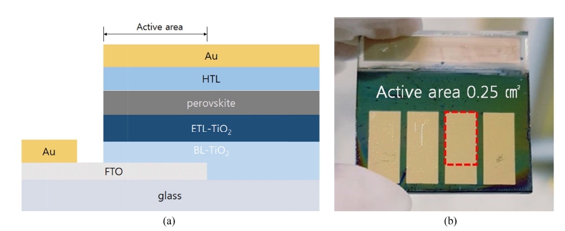
Fig. 1
(a) Illustration of the cross-sectional structure of the proposed PSC and (b) an optical image of a perovskite solar cell.
To fabricate these devices, a cleaned glass/500 nm FTO substrate with dimensions of 25 × 25 × 2.3 mm3 (width, height, and thickness, respectively) was prepared. To produce the BL, after an ultraviolet(UV)/O3 treatment, a compact TiO2(Sharechem, SC-BT060) solution was spin-coated at 2,800 rpm for 20 s, followed by heattreatment on a 125 ºC hot plate for 5 min, thus forming a glass/FTO/BL-TiO2 structure. To form the meso-TiO2 layer, 360 mg of 20 nm(Dyesol, 18NR-T) and 30 nm (Dyesol, 30NR-D) TiO2 pastes were separately diluted in 3 ml of ethanol. Portions of these paste samples were then mixed at a 1:1 ratio to prepare a blended solution. After spin-coating the prepared dilution at 4,000 rpm for 30 s, it was sintered at 500 ºC for 30 min, thereby obtaining a glass/FTO/BL-TiO2/20 nm, 30 nm, or mixed TiO2 layer structure. The same method reported by K. Kim et al.13) was then used to fabricate subsequent layers, finally producing PSC devices consisting of a glass/FTO/BLTiO2/ 20 nm, 30, nm or mixed TiO2/perovskite/HTL/80 nm Au electrode structure.
The microstructure of the fabricated TiO2 its the surfaces and cross-sections were analyzed using FESEM( SU-8000, Hitachi) at an acceleration voltage of 5 kV. To compare the pore characteristics according to the TiO2 particle size, the Brunauer–Emmett–Teller(BET) method(3Flex, Micromeritics) was used. Specifically, the pore volume and pore size were analyzed by injecting N2 gas at 200 ºC, and the gas adsorption was evaluated.
Absorbance of the prepared PSC device was analyzed by ultraviolet-visible-near-infrared(UV-VIS-NIR) spectroscopy( UV3105PC, Shimadzu) with an absorption-mode apparatus by slit 20 and medium scan speed. Mean absorbance in the visible-light region of 400-800 nm was obtained by adding the absorbance at each wavelength and dividing it by the number of added times. To examine the photovoltaic properties of the PSC device, current– voltage(I–V) were recorded using a solar simulator(PECL11, Peccell) and a potentiostat(compactStat.h, Ivium). Through the I–V analysis, the short circuit current density (Jsc), open circuit voltage(Voc), fill factor(FF), and ECE were calculated. Furthermore, to examine their long-term stabilities, changes in the FF and ECE were observed for 360 h.
3. Results and Discussion
Fig. 2 shows the images of the surface and crosssectional microstructures of the glass/FTO/BL-TiO2/20 nm, 30 nm or mixed TiO2 devices. Fig. 2(a) shows a magnified image of the 20 nm TiO2 surface. An analysis of this image confirmed that TiO2 formed a mesoporous layer with a thickness of about 218 nm and an average particle size of 20 nm.
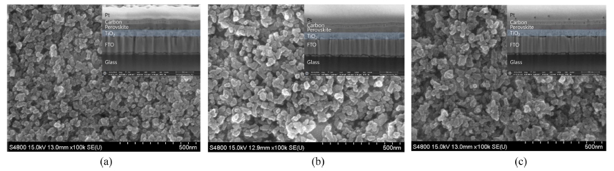
Fig. 2
FE-SEM surface and cross-sectional (inset) images of (a) 20 nm, (b) 30 nm, and (c) mixed TiO2.
Fig. 2(b) shows an image of a 30 nm TiO2 surface, which was magnified and analyzed in the same manner as that in Fig. 2(a). The results confirmed that TiO2 and an average particle size of 30 nm formed a mesoporous layer with a thickness of about 214 nm.
Fig. 2(c) shows an image magnified and analyzed for the TiO2 surface that was fabricated by mixing 20 and 30 nm TiO2 at a 1:1 ratio; the results confirmed that spherical TiO2 with an average particle size of 25.2 nm formed a mesoporous layer with a thickness of about 210 nm.
Therefore, the microstructures of the TiO2 layers fabricated using 20 nm, 30 nm, and mixed TiO2 confirmed that regardless of the particle size, mesoporous TiO2 layers with similar thicknesses formed.
Table 1 shows the pore volumes and pore sizes based on the BET analysis results according to the TiO2 particle size. The analysis results confirm that the pore volumes and pore sizes were all similar, regardless of the TiO2 particle size. This is consistent with the results of the SEM analysis, in which the structures were all similarly formed regardless of the TiO2 particle size. Thus, the pore sizes were determined to all be similar because the difference in TiO2 particle size was only 10 nm, which is extremely small.
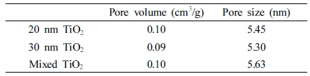
Fig. 3 shows the measured absorbance of devices fabricated using the glass/FTO/20 nm, 30 nm, or mixed TiO2/perovskite structure within the visible region of 400 to 800 nm. In the upper-right corner, absorbance within the 570 to 600 nm range is magnified. From 400 to 500 nm wavelength, the absorbance of the 20 nm TiO2- employed device was low, and the devices employing 30 nm and mixed TiO2 showed similar absorbance higher than that of the device employing 20 nm TiO2. In the range of 500-750 nm wavelength, 30 nm TiO2 maintained the highest absorbance, as shown in the magnified image of the 570-600 nm range in the upper-right corner, followed by 20 nm and mixed TiO2 in that order.
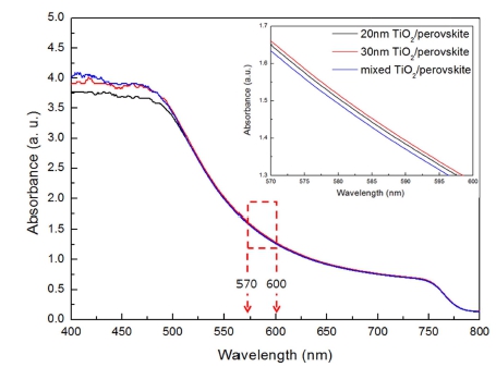
Fig. 3
UV-VIS-NIR absorbance spectra according to TiO2 particle size. Inset shows a magnified view of the range from 570 to 600 nm.
The sum of absorbance in the range of 400-800 nm was divided by the number of measurements to obtain the arithmetic mean. The results confirmed that the mean absorbance of 20 nm, 30 nm, and mixed TiO2 was 1.820, 1.870, and 1.868, respectively; thus, the mean absorbance was determined to be similar within the margin of error.
Fig. 4 shows I-V data for the PSC device according to the TiO2 particle size. The Jsc is known to be affected by the light intensity.14) The Jsc of the PSC devices employing 20 nm, 30 nm, and mixed TiO2 were recorded to be 19.09 mA/cm2, 20.34 mA/cm2, and 19.21 mA/cm2 respectively. This result follows the same trend as the aforementioned absorbance result, and they were determined to be identical within the margin of error.
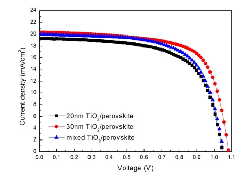
In the case of Voc, which is determined by the band gap of the material, the devices employing 20 nm, 30 nm, and mixed TiO2 all showed an excellent Voc of higher than 1.00 V. It was therefore determined that this result was obtained because they all used the same material.
In the case of FF, the value 0.58, 0.70 and 0.60 were confirmed for employing 20 nm, 30 nm, and mixed TiO2, respectively. Such an FF is known to be affected by the series resistance of PSC,14) and it was determined that the reason why the FF was lower in the 20 nm or mixed TiO2-employed device than in the 30 nm TiO2-employed device was because the respective resistances of the TiO2 themselves were different.
Therefore, based on the Jsc, Voc, and FF results, the highest ECE of 15.07 % was confirmed in the 30 nm TiO2-employed PSC. This result was due to the difference in FF caused by the difference in particle sizes of the 20 nm, 30 nm, and mixed TiO2.
Fig. 5 shows the changes in FF and ECE over a 360 h period for devices fabricated using glass/FTO/20 nm, 30 nm, or mixed TiO2/perovskite/HTL/Au structures.
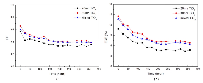
Fig. 5(a) shows the FF data, which are most directly related to the ECE among the photovoltaic properties, according to the TiO2 particle size. Initially, FF was highest for the 30 nm TiO2, as confirmed by the shape of the I-V curve in Fig. 4. Over time, however, FF decreased similarly, regardless of the TiO2 particle size.
Fig. 5(b) shows the ECE over time according to the TiO2 particle sizes. The ECE decreased over time, which is identical to the FF trend demonstrated in Fig. 5(a). Considering that there was no difference between the surface and cross-sectional microstructures of the TiO2 particle sizes, as confirmed in the microstructure results discussed earlier, and there was no difference in most of the photovoltaic properties, the difference in the ECE was determined to be caused by the difference in the respective resistances according to the TiO2 particle sizes.
Fig. 6 shows schematic one-dimensional models of TiO2 particles with 20 nm, 30 nm, and mixed diameters. Together with the photovoltaic results above, and assuming that the TiO2 layers all have the same thickness, these models illustrate the resistance to electron movement according the particle sizes. Here, electrons can be considered to move through the PSC along a path directly through the perovskite layer and a path the through TiO2 layer. All paths through the perovskite layers can be considered to be identical, regardless of the TiO2 particle size.
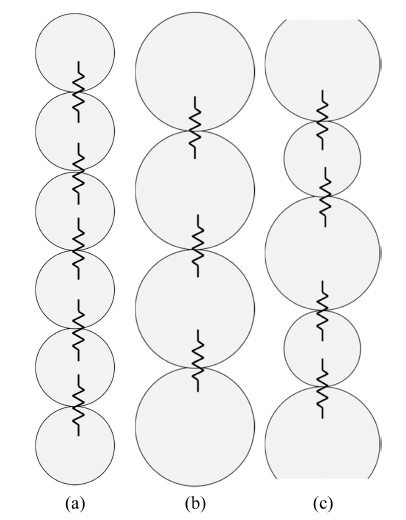
Fig. 6
Simplified one-dimensional series resistance model of (a) 20 nm, (b) 30 nm, and (c) mixed TiO2.
Fig. 6(a) shows the resistance of the electrons moving through the TiO2 from the upper part to the lower part in the device that employed 20 nm TiO2. This model assumes that all the interfaces between TiO2 and TiO2 behaved as resistors, thus hindering electron movement. Based on this assumption, along the same length, 20 nm TiO2 provides five interfacial resistors, whereas Fig. 6(b) and (c) show three and four interface resistors, respectively, using the same model.
Using such a one-dimensional model, the overall interfacial resistance of the TiO2 layer can be predicted to increase as the particle size decreases because of the increased interfacial resistance of electrons moving through the TiO2. Such an increase in the interfacial resistance directly decreases the FF, and such a trend is consistent with the FF results of the PSC confirmed earlier.
Therefore, as the nano-TiO2 particle size decreases, the resistance of the TiO2 layer increases, thus increasing the series resistance of the entire PSC device and decreasing the FF of the PSC device. Thus, the ECE also decreases with decreasing particle size.
4. Conclusions
PSC devices employing TiO2 of different particle sizes of 20 nm, 30 nm, and a 1:1 mixture were fabricated, and their microstructures and photovoltaic properties were compared. Microstructural observations confirmed that a mesoporous TiO2 layer with a 210 nm thickness was similarly formed, regardless of the particle size. The photovoltaic characterization showed that the absorbance was similar for the 20 nm and 30 nm TiO2 layers. The ECE result was highest in the device with a particle size of 30 nm, and the FF changes of the PSC device according to the particle size had an effect on the ECE. A one-dimensional model of the resistance in the TiO2 layer determined that the interfacial resistance, which hinders electron movement, varies depending on the particle size. Ultimately, the smaller the particle size is, the higher is the interfacial resistance, which may be the major cause of the lower FF and ECE.