

1. Introduction
Magnons are collective excitations of spin waves in magnetically ordered materials.1) A magnon spin current refers to the flow of magnons, quanta of spin waves, through a magnetic material. Differing from electron spin current, magnon spin current can propagate in an insulator with no charge carrier (electrons), avoiding energy dissipation in modern electronic devices caused by Joule heating.2) Furthermore, the magnons provide long-distance spin information propagation (up to millimeters) in low magnetic loss materials such as yttrium iron garnet, Y3Fe5O12 (YIG).3) Besides, magnons and electron spin currents can be interconverted to each other via spin pumping and spin transfer torque.4) Details, a magnetic material undergoes a magnetic resonance or thermal excitation, causing its magnetization to precess. The precession generates magnons, which can inject an electron spin current into the adjacent layer when they come into contact with a nonmagnetic conductor.5) This is called the spin pumping process. For the reverse process, when an electron spin current is injected into a magnetic material, the angular momentum carried by the spin current can exert a torque on the magnetization of the magnetic material.6) This torque can excite the magnetic moments, resulting in the generation of magnons, a phenomenon referred to as spin-transfer torque. All aforementioned characteristics of magnons make it suitable for applications in spintronic devices.4,7,8)
The spin valve, an essential element in memory devices, exploits giant magnetoresistance to control electrical current based on the relative alignment of magnetization in its layers. Its operation primarily depends on spin currents carried by electrons, and as a result, it is composed mostly of metallic layers. However this design is constrained by electrical conduction-related challenges, such as Joule heating loss, low speed, and poor thermal stability. In contrast, the magnon valve (MV), which transmits information via magnons instead of electrons, has recently emerged as a promising alternative for memory device applications. Since MV can be made of magnetic insulators, and magnons possess outstanding properties that they are expected to enable memory devices that operate with lower power, greater stability, and higher efficiency.
Similar to the spin valve, MV is composed of two insulating ferrimagnetic (FM) layers separated by a non-magnetic spacer. Its operation depends on the alignment of the magnetization in the two FM layers. The high and low resistance are corresponded to antiparallel (AP) and parallel (P) states of magnetization in the FM layers. To maximize the MV efficiency, low magnetic damping constant materials such as rare-earth garnets should be used for the propagation of magnons.9,10,11,12) Meanwhile, the spacer layer also plays a very important role in defining the readout signal of the MV. It permits the magnon spin current from an FM layer to pass through and inject into another FM layer. Besides, it should be thick and strong enough to decouple the magnetization between the two FM layers. Recently, only a few materials, such as NiO and Au, have been proposed as MV spacers.9,10,11,12) Hence, there is still a large demand for finding a more prominent material as a spacer to improve the MV operation.
In this study, we present an investigation of the MV properties of the YIG/Pt/YIG structure. Platinum (Pt) was selected as the spacer layer due to its excellent thermal stability, making it suitable for devices operating in high-temperature environments.13,14) Additionally, Pt has a large spin Hall angle, which facilitates efficient magnon-to-spin conversion, allowing magnon-spin currents to propagate effectively through the Pt spacer.15,16) By varying the thicknesses of the YIG and Pt spacer layers, we were able to tune the MV ratio, which correlates with the output signal of the MV.
2. Experimental Procedure
In this study, YIG/Pt/YIG multilayers structure was grown on a (111)-oriented gadolinium gallium garnet (Gd3Ga5O12, GGG) substrate, which was cleaned by ultrasonicating in acetone and ethanol for approximately 30 min each. The preparation of the YIG target was previously described in our earlier work.17) Both the bottom YIG layer (b-YIG, adjacent to the GGG substrate) and the top YIG layer (t-YIG, adjacent to the Pt electrode) were deposited at room temperature (RT) using sputtering in an atmosphere of 22.5/2.5 sccm of Argon/Oxygen. Before sputtering, the chamber was pumped to a base pressure of 6 × 10⁻⁷ Torr using a rotary and molecular pump system. During deposition, a throttle valve was used to maintain a working pressure of 15 mTorr. The RF power and rotation speed were set at 100 W and 10 rpm, respectively. Before the deposition of the spacer Pt (s-Pt) layer, the b-YIG layer was annealed at 750°C for 2 h under a flow of 100 sccm Oxygen. The purpose of this annealing process is to form a high-quality YIG layer with very low coercivity and a smooth surface. The s-Pt layer was then deposited onto the annealed b-YIG layer using DC sputtering at 15 W with a base pressure of 6 × 10⁻⁷ Torr at RT. A 22.5 sccm of Argon was injected continuously to generate plasma under a working pressure of 3 mTorr. The t-YIG layer was deposited under the same conditions as the b-YIG layer onto the s-Pt layer to complete the multilayer structure. Subsequently, the entire structure was annealed at 700°C under the same gas and time conditions as the b-YIG annealing. The lower annealing temperature for the entire structure, including the Pt and t-YIG layers, was chosen to preserve the structural integrity of the Pt film. Furthermore, this lower annealing temperature resulted in a reduced quality of the t-YIG layer, which is beneficial for enhancing the coercivity of t-YIG compared to b-YIG, thereby promoting a clearer magnetization reversal (MV) state (to be discussed in detail later).
The MV effect of the samples was investigated through the spin Seebeck effect (SSE), for the readout process of MV, using customized SSE system details described in our previous report.18) For the SSE measurements, an electrode Pt (e-Pt) layer was deposited onto the t-YIG layer using a shadow mask with dimensions of 3 × 6 mm2, following the same sputtering conditions as those used for the s-Pt layer.
The magnetic and structural characterizations were performed via vibrating sample magnetometry (VSM; model US/7407, Lake Shore Cryotronics, USA), X-ray diffraction (XRD; model D8 HR-XRD, Bruker, USA), respectively. The crystallinity quality of the samples was determined via high-resolution transmission electron microscopy (TEM; model JEM-ARM200F, JEOL, Japan).
3. Results and Discussion
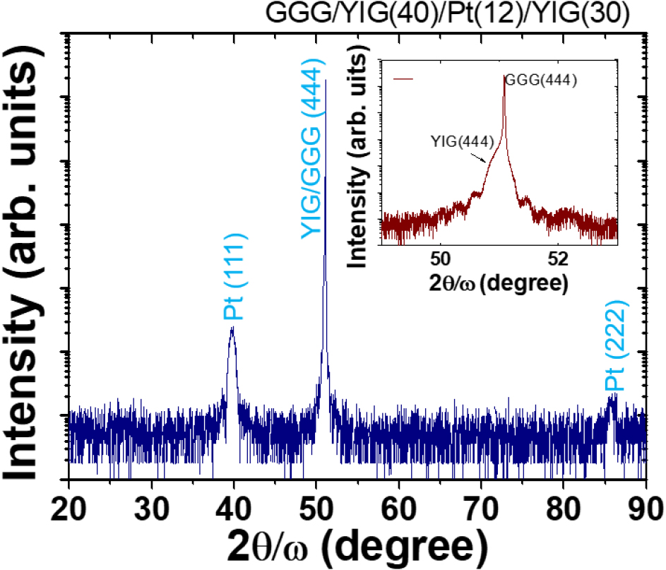
To confirm the growth of the GGG/YIG/Pt/YIG MV structure, we first investigate the crystallinity of our sample using the XRD technique. Fig. 1 presents the high-resolution XRD pattern of the GGG/YIG(40)/Pt(12)/YIG(30) sample (unit in nm). The peaks observed at 39.8° and 85.6° correspond to the (111) and (222) crystal planes of Pt, respectively. This proves the presence of Pt in our MV. The GGG/YIG(444) peak, which is located at around 51°, is clearly shown in the narrow scan XRD pattern (inset figure). Besides, the Laue fringes were also observed indicating the well-layered growth of the YIG films. No other YIG peaks are observed, implying that YIG prefers to grow along the (444) direction. Furthermore, there is no existence of any other XRD peaks confirming the high crystallinity along the sample’s normal direction.
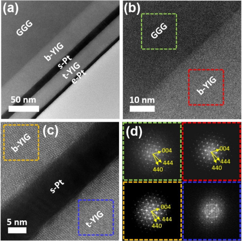
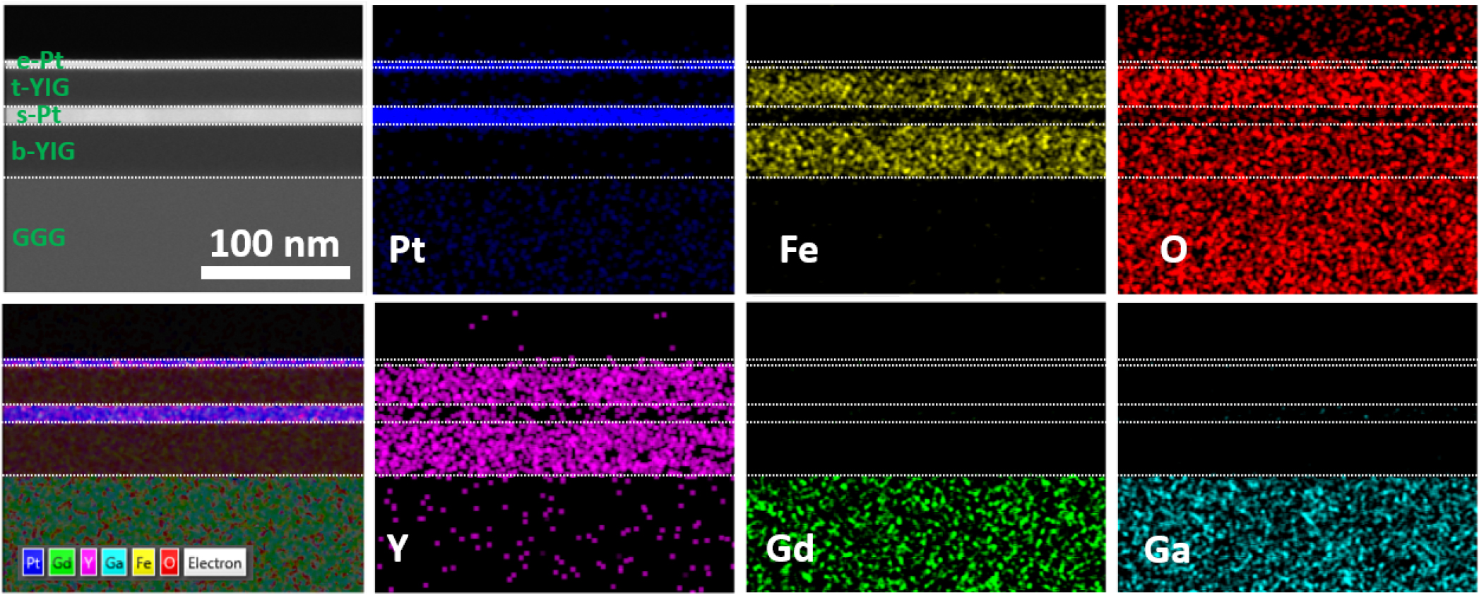
For the detailed structural analysis, TEM was employed to the same sample e.g., [GGG/YIG(40)/Pt(12)/YIG(30)]. The TEM specimen was prepared via focused ion beam (FIB) lithography from a 1 cm2 sample. Cross-sectional TEM images [Fig. 2(a)] confirm the layer-by-layer arrangement and the thickness of each layer, with clear interfaces observed between b-YIG/s-Pt and s-Pt/t-YIG in Fig. 2(b, c). Fast Fourier transform (FFT) patterns from high-resolution TEM (HR-TEM) images of the YIG layers [Fig. 2(d)] reveal that the atomic structure of b-YIG is identical to that of the GGG substrate (i.e., single crystaline), while t-YIG exhibits a different structure with a signal of amorphous or polycrystalline phase (visible as a bright ring in FFT), undetectable by XRD. Given the high-temperature annealing step in sample fabrication, interdiffusion of elements could be a concern. To assess this, energy-dispersive X-ray spectroscopy (EDX) was used for elemental mapping (Fig. 3), confirming the uniform distribution of Gd, Ga, Y, Fe, O, and Pt without any interdiffusion. The results show that the layer-by-layer structure is maintained both physically and chemically, even after annealing at 700°C.
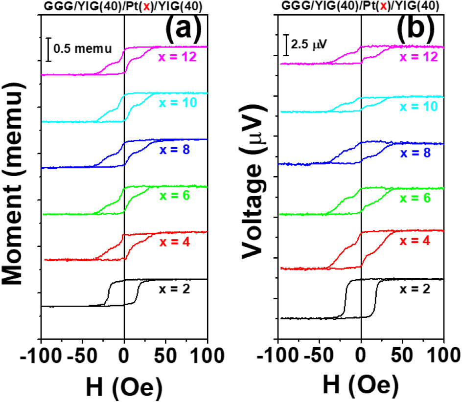
In the MV, the spacer plays a very important role in decoupling the exchange interaction between the magnetization of FM layers and hence in the MV ratio.9) Therefore, we first fabricate the YIG/Pt/YIG structure with changes in the s-Pt thickness (ts-Pt) and investigate its properties by VSM measurement as shown in Fig. 4(a). For 2 nm of ts-Pt, there is strong exchange coupling between two YIG layers thus we can observe only a single transition of the total magnetization. As thickness increased, the exchange coupling became weaker and then we could see the separation switching of the magnetization which is important for defining clear P/AP states of the MV reading signal. The lower coercive field transition corresponds to the switching of b-YIG magnetization, while the larger one belongs to t-YIG magnetization. As discussed in the TEM result, the crystallinity of b-YIG is higher than that of t-YIG, resulting in a lower coercivity.10,17,19) Consequently, in the case of the 2 nm-thick s-Pt layer, the magnetization switching appears to be predominantly governed by t-YIG, which exhibits a higher coercivity. We then measured the SSE voltage for this sample set with results shown in Fig. 4(b). It is worth noting that the VSM measurement detects the volumetric magnetization signal. It means that the VSM detects 100 % signal of the magnetization in the MV regardless of the ts-Pt. Meanwhile, the SSE measurement, which directly represents the reading process of the MV, detects only the magnon spin current arrived in detection layer. The SSE signal of the detection layer is composed of two magnon spin current i.e. the magnon spin current from the b-YIG (ηb-YIG) and t-YIG (ηt-YIG) layers which are generated under a thermal gradient. The ηb-YIG has to pass through the s-Pt and t-YIG layers to be injected into e-Pt and contribute to the SSE signal. Therefore, the SSE signal is sensitive to the ts-Pt. Here, we observed similar magnetic and SSE hysteresis loops implying that the ηb-YIG can partially arrive at the e-Pt layer and contribute to the SSE signal for all samples. There is a small difference in the coercivity for the magnetic and SSE hysteresis loops. It could be the difference in the uncertainty and alignment of Gaussmeters which are used to control the field in VSM and SSE systems.
The MV ratio (RMV) can be defined as (VP / VAP) × 100 % where VP and VAP are the measured SSE voltage at which magnetization of b-YIG and t-YIG are parallel and AP, respectively. The parallel (green region) and (purple region) AP magnetization states are determined by 1st derivative of the SSE voltage to the applied magnetic field.11)Fig. 5(a) shows the SSE hysteresis loop and its 1st derivative curve of the GGG/YIG(40)/Pt(12)/YIG(30) sample. The sharp peaks close to the zero field correspond to the switching process of the b-YIG layer. Meanwhile, the broad peak at the larger field belongs to the change in the t-YIG magnetization state. Because the bottom YIG was grown directly on GGG substrate and annealed at a higher temperature (i.e., 750 °C) leading to high quality (as seen in Fig. 2) and low coercivity of YIG. Meanwhile, t-YIG which was grown on s-Pt has a poorer crystal structure (as shown in the TEM result) and also magnetic properties. Aside to RMV, the clarity of the P and AP magnetization states is another important parameter of the MV. In order to quantify the separation of P and AP state, we have calculated the half width at half maximum (HWHM) of top magnetic layer and peak-to-peak separation of two magnetic layers. The separation of P/AP two states (S) can be defined as (Hpp / HHWHM(t-YIG)) × 100 % [Fig. 5(a)]. Here, Hpp is distance from the sharp and broad peaks in the same corner in the quadrant. And HHWHM(t-YIG) is the HWHM of the t-YIG magnetization transition. The HHWHM(t-YIG) is taken because it is always larger than HHWHM(b-YIG) which mainly affects to the separation of P/AP states. The larger S value gives a clear separation of two P/AP states meaning that independent magnetization control can be achieved.
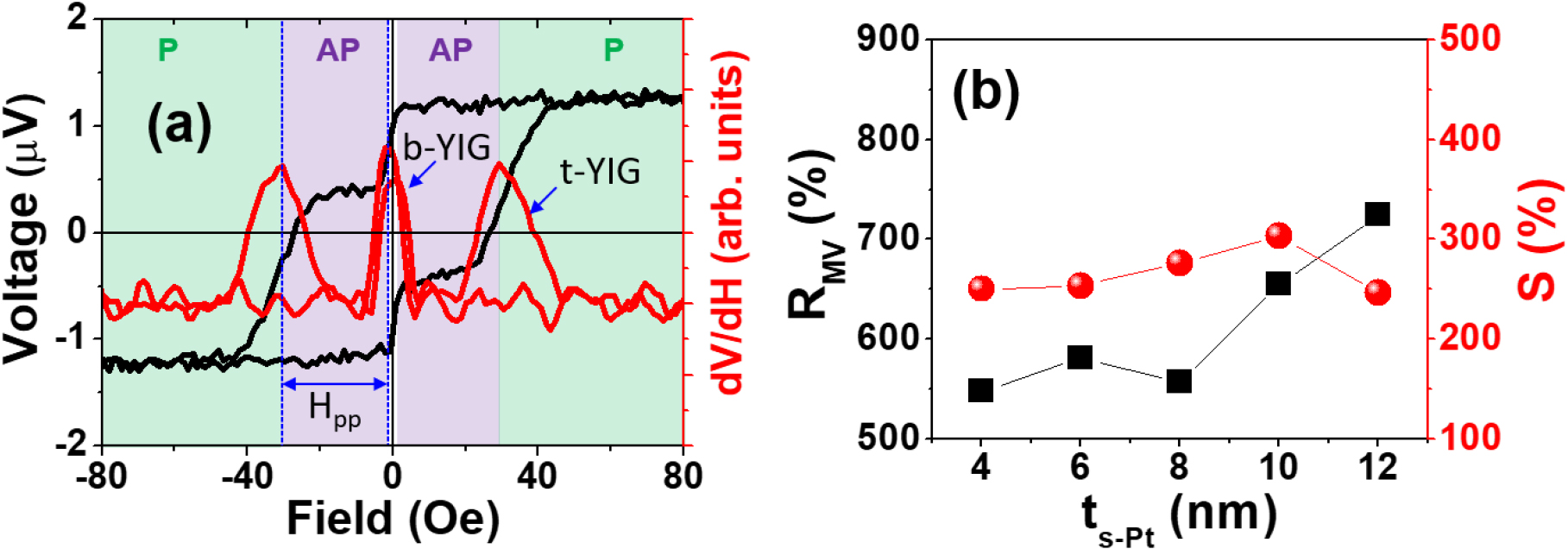
Based on the definition of RMV and S, we calculated these parameters for various s-Pt samples, as shown in Fig. 5(b). Basically, the MV signal is influenced by the magnitude of ηb-YIG and ηt-YIG and their relative amplitudes injected into the e-Pt layer. In other word, VP / VAP is proportional (ηb-YIG + ηt-YIG) / ηt-YIG which means the RMV is decreased (increased) when ηt-YIG (ηb-YIG) increased. In this sample set, the ηb-YIG is almost identical to all samples since the thickness of b-YIG (tb-YIG) are the same and all grown directly on the GGG substrate. From TEM and EDX results, we found that there is no diffusion of the Pt. Therefore, we can assume that the quality of the Pt layer in different samples is also the same. The ηb-YIG driven by a thermal gradient, is injected into the s-Pt layer, where it is converted into an electron spin current at the b-YIG/s-Pt interface and reconverted to a magnon spin current at the s-Pt/t-YIG interface.10) Given that the Pt thickness is larger than the spin diffusion length,20) the magnon spin current can be dissipated partially. The magnon spin dissipation rate is increased as the ts-Pt increases. After passing through the s-Pt, the ηb-YIG keeps continuing to diffuse through the t-YIG layer and be converted to electron spin current which contributes to the generation of SSE voltage via inverse spin Hall effect (ISHE). However, the dissipation rate of the magnon spin current is also dependent on the quality of the t-YIG film related to the magnon propagation length. Meanwhile, the quality of YIG can be affected by the ts-Pt because it hinders the lattice-matching growth mode for the t-YIG. In detail, with thinner Pt, t-YIG can be grown partially following the b-YIG layer and vice versa. While the growth is gradually reduced as ts-Pt is increased. Thus, the crystal quality of t-YIG is degraded as s-Pt becomes thicker. As a minor summary, ts-Pt enlarges the magnon dissipation rate in t-YIG and in s-Pt itself. Additionally, the exchange interaction between the magnetization of the b-YIG and t-YIG becomes an important factor that defines the RMV as well as the C of the MV. As we can see P and AP states can not be defined for a 2 nm-thick s-Pt sample with strong exchange coupling between two YIG layers causing a single magnetization transition under the external magnetic field (as observed in VSM hysteresis loop). When the ts-Pt increases up to 4 nm, this exchange coupling reduces mostly. As mentioned above, the quality of t-YIG is related to the dissipation rate of ηb-YIG. It means the RMV would be decreased as the ts-Pt increases since the ηt-YIG contributing to VAP become larger. Otherwise, the quality of t-YIG layer also decides how large ηt-YIG can be generated. As the quality of YIG decreases, the ηt-YIG is also decreased. Hence the RMV should be decreased as ts-Pt decreases because RMV is inversely proportional to ηt-YIG.10) Since the RMV increases as the thickness of the s-Pt increases from 6 to 12 nm, the effect of t-YIG quality on the ηt-YIG seem to be larger than that of magnon spin dissipation rate inside s-Pt and t-YIG. The separation of two states S increases as the s-Pt size grows up to 10 nm, but decreases once s-Pt exceeds 10 nm. However, the variation of the S is much smaller than that of the RMV. Therefore, the sample with ts-Pt = 12 nm is the optimal condition for large MV efficiency.
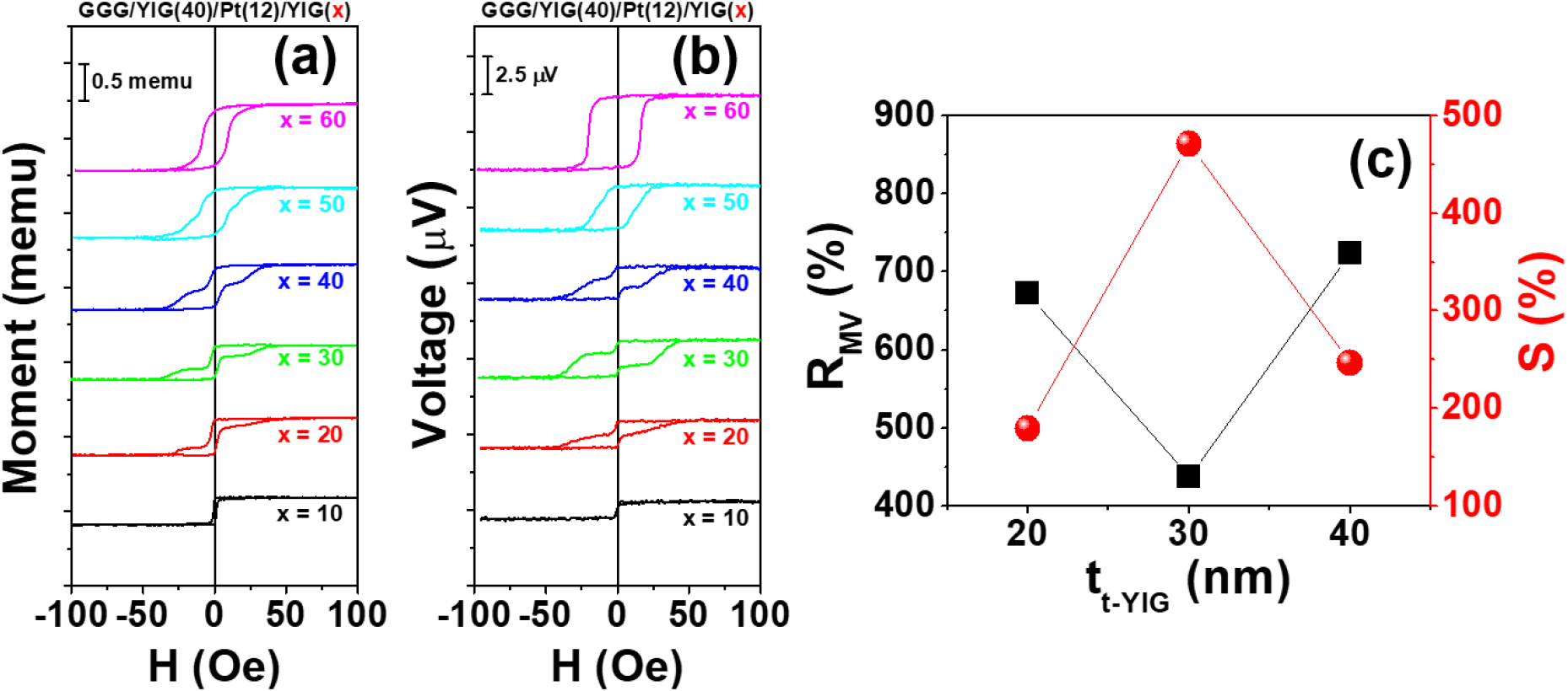
Not only ts-Pt but also the thickness of YIG layers can affect the MV properties. Hence, we fixed the ts-Pt of 12 nm at which the magnetization of b- and t-YIG layers are well decoupled. First, we varied the thickness of the t-YIG layer (tt-YIG) and then characterized the samples of which the result is shown in Fig. 6. We observe that as the tt-YIG is increased, the magnetic moment of the sample is also increased, demonstrating the well deposition of the YIG films. With the thinnest tt-YIG e.g., 10 nm case, the signal of the b-YIG layer is almost dominant for both magnetic and SSE hysteresis signals. As the tt-YIG further increases, both YIG layers’ signal can be observed. However, if tt-YIG becomes thicker than 40 nm, the signal from t-YIG becomes dominating. For these samples, the RMV and S can not be defined from the SSE hysteresis loops. The extraction of RMV and S for other samples are plotted in Fig. 6(c). From this figure, we can observe that with tt-YIG = 30 nm, the MV states are very clear with a high value of S while the RMV is the smallest among samples. There could be a trade-off between the RMV and S at a certain tt-YIG of 30 nm. We should figure out which condition is better for MV efficiency. We can see that sample with tt-YIG = 40 nm has a higher RMV and S than that of the sample with tt-YIG = 20 nm. However, the factors of sample with tt-YIG = 30 nm needs to be considered separately. There is enhancement of 1.91 for S of sample 30-nm tt-YIG compared to sample 40-nm tt-YIG. Meanwhile, only 1.66 times of the enhancement for RMV of 40 nm-thick t-YIG compared to that of 30 nm-thick t-YIG. Therefore, from the benefit point of view, a sample with tt-YIG = 30 nm is the optimal condition.
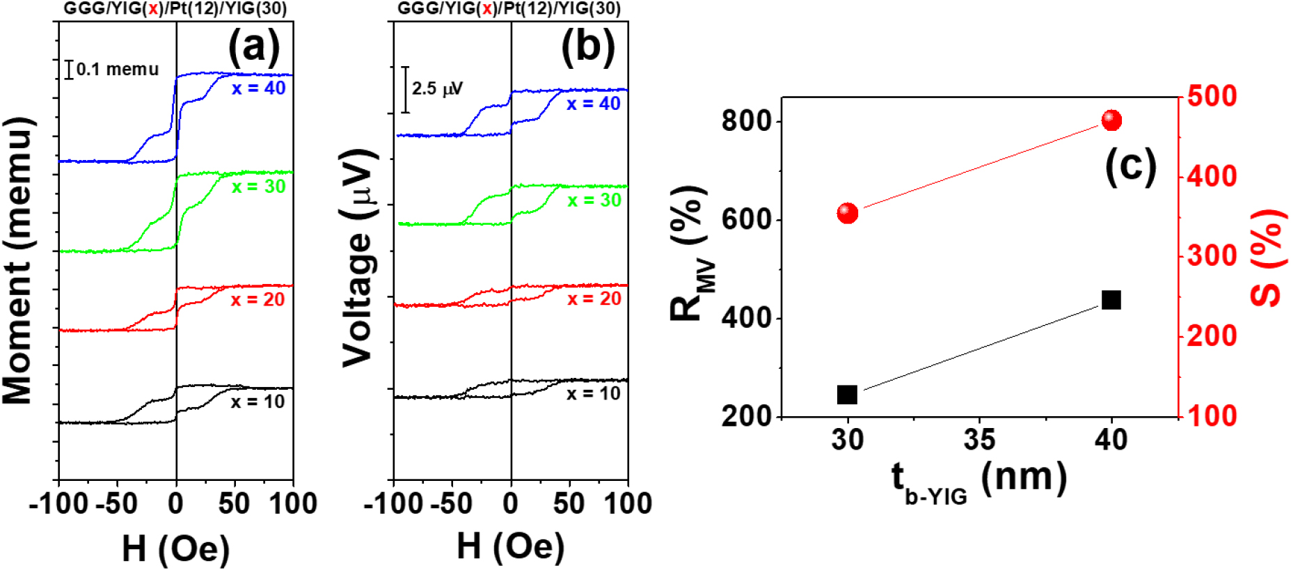
Finally, we studied the effect of the tb-YIG on the MV properties. For this purpose, we fix the ts-Pt and tt-YIG of 12 and 30 nm, respectively. From the VSM measurement [Fig. 7(a)], we observe the increase of the low coercivity portion in the magnetic hysteresis loop as the tb-YIG is thicker. There is a similar trend happened in the SSE hysteresis loop [Fig. 7(b)] but with a different ratio. With tb-YIG of 10 and 20 nm, the SSE signal is dominated by the t-YIG even though in the magnetic hysteresis loop we can see the contribution of the b-YIG layer. Because in SSE voltage, ηb-YIG is dissipated in s-Pt and t-YIG partially causing the insignificant contribution to the ISHE. Therefore, we can not determine the RMV and S for these samples via a derivative of the SSE signal. For thicker tb-YIG, these values can be defined and plotted in Fig. 7(c). As we expected, the RMV is increase when tb-YIG gets thicker. Because thicker tb-YIG enlarges the ηb-YIG, consequently boosts the RMV. Similarly, the S is also increased significantly when tb-YIG = 40 nm. In summary, from the whole experimental parameters study, we obtain the optimal MV structure of GGG/YIG(40)/Pt(12)/YIG(30) with RMV = 436.6 and S = 471.3 %.
4. Conclusion
We have successfully grown the MV of the GGG/YIG/Pt/YIG structure with clear separation of two P/AP states which is crucial for the operation of the MV. We found that the thickness of s-Pt and two YIG layers affect strongly the MV properties. Especially, the thickness of s-Pt is plays a important role not only to decouple the magnetic states but also to diffuse the magnon current from bottom magnetic layer to top magnetic layer. By optimizing the thickness of layers, we can obtain with RMV = 436.6 and S = 471.3 % for the structure of GGG/YIG(40)/Pt(12)/YIG(30).
