

1. Introduction
In terms of the structural design, the crystalline Si solar cells can be broadly defined as front-lit and back-lit. The dominant design is the front-lit where the incident light or photons enter the surface close to the pn junction. Here, the base (substrate) is usually p-type, and the thin emitter layer on top is n-type. The cathode electrode is shaped as fingers or a grid to allow in the light and contacts the emitter. The anode electrode contacts and fully covers the bottom of the substrate. The alternative back-lit or BCBJ (Back Contact and Back Junction) configuration puts both cathode and anode on the backside (formerly the front side in case of the front-lit) of the solar cell. This leaves the front surface (formerly the backside in case of the front-lit), which faces the sun, completely denuded of metal electrodes.
The reason behind the fact that the substrate is normally p-type and the thin emitter layer is normally ntype is because the minority carriers in the thick p-type substrate are electrons that travel faster than holes, so that the electrons reach the n-type emitter much more readily than when the situation is the opposite, where the substrate is n-type and the thin emitter is p-type. The downside of having p-type as the substrate is that the majority carriers are holes, the slower carriers, which means that the resistivity is proportionately higher that results in the current and power loss in the substrate.
In order to better comprehend the physical differences between the two designs and moreover the operational principles of the solar cell in general, it is useful to draw analogies between the solar cell and its larger twin, the waterfall. The analogies can be seen by the fact that electrons are lifted to the conduction band and gain potential energy by solar energy and then release the potential energy as they return to the valence band, just as water molecules are lifted to the air (vaporized) and gain potential energy by solar energy and then release the potential energy as they return to the sea. Stiff potential gradients at the pn junction and at the waterfall itself allow a quick release of the potential energy that provides the driving force and kinetic energy for conduction electrons as well as water molecules. In this regard, one would make a great solar cell if all the attributes that make a great waterfall are incorporated in solar cell design.
Looking at the solar cell or the pn junction and the waterfall as analogical twins, the front-lit design allows the electron-hole pairs (rain) form very near or on the pn junction (waterfall), enabling a rapid electrical current (water) flow from the p-type to the n-type. As in this design the cathode is formed on the front emitter surface and gridded, the downside of the front-lit design is that the gridded cathode reflects the incident light where the light meets its metallic surface and thus causes shading, i.e., a loss of light flux into the solar cell. Depending on the grid design, the shading may account for as much as 10 % loss in light influx. This translates into a 10 % loss in the output power of the solar cell, or a 2 % loss in the energy conversion efficiency in the standard 20 % efficient solar cell. In the back-lit or BCBJ solar cells, the shading is absent as both cathode and anode are placed on one side and the other side is completely free and denuded of electrodes. The downside of the BCBJ configuration is that the incident photons are absorbed and generate electron-hole pairs very far away from the pn junction. This is like the rain (electron-hole pairs) is falling on the far upstream from the waterfall (pn junction). Like the rainwater, due to seepage, that may not necessarily all reach the waterfall, the minority-carriers, due to recombination with majority carriers, may not all reach the pn junction. As such, the BCBJ (back-lit) design ordinarily yields less power output than the comparable front-lit design. Another inconvenience is that the emitter layer and the cathode need to be patterned to give rooms to the anode to contact the substrate.
Despite the downside and inconvenience mentioned, the BCBJ design holds greater promise now as the crystal growth methods and wafer fabrication technologies improve. That is, improvement in Czochralski or float-zone crystal growth method results in better quality Si crystals, and improvement in wafer fabrication technologies results in ever thinner substrates. With better quality materials, the minority carriers have longer mean free lifetimes, i.e., less likely recombine with majority carriers, enabling them to travel longer distances to reach the pn junction and respective electrodes. With thinner substrates, the distances to the pn junction and respective electrodes are proportionately shorter, enabling the minority carriers reach them faster.
In regards to energy conversion efficiencies, for frontlit Si solar cells, the highest efficiency reported to date for an actual cell is 24.7 % by a method known as PERL (Passivated Emitter, Rear Locally-diffused),1) while the more typical value accepted in laboratory-scale solar cells is about 20 %, or 20 mW·cm−2 under AM1.5.2) As for back-lit or BCBJ Si solar cells, the efficiency was somewhat lower, but has been fast approaching that of the front-lit solar cells and lately has pulled nearly even at as high as 21.5 % with float-zone Si substrates,3) thanks to the improvements in material quality and wafer fabrication just mentioned above.
As the material cost consideration encourages the switch from more expensive float-zone or Czochralski monocrystalline silicon to a variety of less expensive polycrystalline silicon, the substrates obviously need to be made thinner in order to deal with the minority-carrier recombination issue. As to exactly how much, as well as the inter-relationship between minority-carrier lifetime and substrate thickness as they together affect the energy conversion efficiency, is a question that can only be answered by repetitive experiments that are yet to be conducted comprehensively. In this work, computer simulations were conducted in lieu of laboratory experiments by using Medici, 2-dimensional semiconductor device simulation software. Despite the virtual nature of computer simulation, the results should prove to be useful in better understanding the substrate issues and serving as a guide in determining the proper substrate quality/thickness combinations for the BCBJ Si solar cells.
2. Experimental
Computer simulation is useful when and where laboratory experiments are too costly and/or time-consuming to the extent that they are not practical. Situations that call for repeated measurements with incremental changes in inter-related variables can be very complex. In the present case of Si solar cells where the substrate thickness and minority-carrier recombination lifetime interact to affect the photovoltaic power generation, the computer simulation is a good option before delving into repeated laboratory experiments. Just as a scaled-down and simplified version of a physical structure, such as house or bridge, can be made to get a good feel of what the real structure would be like, a graphic version of a solar cell can be made in the virtual space and all the essential variables can be tested in computer simulation.
In the present study, a commercially available 2-dimensional device simulation software called Medici is utilized to investigate the BCBJ design. The Medici simulation consists of four major steps. First, the solar cell structure is formed by grids or mesh, a sort of like building a modeled house using match sticks. The regions near the front and back surfaces and at the pn junction where active photo-generation and carrier recombination occur are finely meshed, and the bulk region deep in the body of the solar cell, where the electrical activities are relatively minor, are coarsely meshed to save computation time. Each type of the n- and p-type regions is then doped to a desired level. Second, the physical models relating to the operation of the solar cell and mathematical models and methods relating to numerical calculations are each specified. Third, the solutions are reached by iterative numerical calculations. Fourth, the simulation results or the outputs are accessed in texts, graphs or other pictorial forms.
The solar cell chosen for the simulation study is a BCBJ structure of p-type silicon substrate. A standard 2- dimensional BCBJ grid structure in the Medici operational manual4) is used and modified as needed. In this BCBJ structure, the substrate, the thickness of which is an independent variable, is doped p-type in the concentration of 1 × 1014 cm−3. Laterally, only a 10 μm segment of the substrate is chosen to conserve the simulation time. The n-type emitter on top is doped to the concentration of 1 × 1017 cm−3. The location of the pn junction, between the emitter and the substrate, or base, is 2 μm below the surface, in this case the back surface. The emitter is patterned as such it occupies about 7.5 μm of the 10 μm device width. The metal electrodes are also patterned as such they provide contacts to the n-type emitter and the p-type base separately. The said grid structure is shown in Fig. 1 and has been used successfully in a previous study concerning a general survey of back-lit (BCBJ) solar cells in reference to a standard front-lit solar cell.5) In the study, a broad investigation of BCBJ parameters, such as incident photon wavelength, angle of light incidence, substrate thickness, emitter width, substrate doping concentration, and emitter doping concentration, was conducted to see how the BCBJ design measure up against the standard front-lit design, and the result showed that the BCBJ design could perform up to 85 % of the front-lit design in terms of the cell power output.
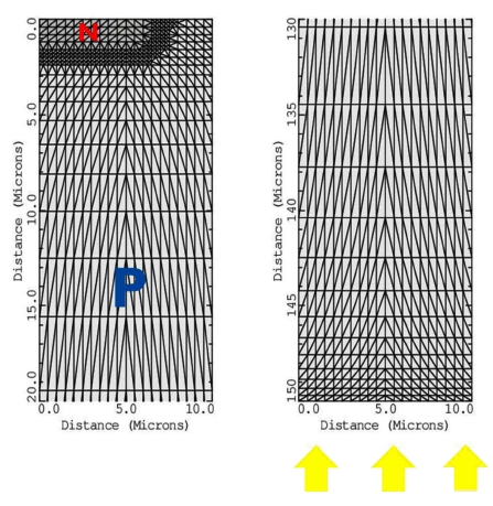
Fig. 1
A typical 2-dimensional grid structure of a BCBJ (back-lit) solar cell rendered by Medici.4) The left shows top 20 μm: the emitter-base np junction is located 2 μm below the top surface. The right shows bottom 20 μm. The light beams are directed normal to the bottom surface.
In regards to model and parameter selection, Auger and concentration-dependent Shockley-Read-Hall recombination models and a concentration-dependent mobility model are chosen. The 2-carrier Newtonian iteration is chosen as the mathematical model in solving the governing equations by finite element analysis. Lastly, except for the parameters that are chosen, default values are used for all others.
The photo-generation rate, electron-hole-pairs·cm−3·s−1, is an exponential function of distance y from the surface and can be expressed as
where FLUX is defined as the photon flux (photons·cm−2 ·s−1) and Y.CHAR is defined as the absorption distance (μm).4) The photon absorption is strongly frequencydependent. That is, higher the frequency, or shorter the wavelength, the stronger the photon absorption and therefore the shorter the absorption distance. For the present simulation experiments, the wavelength of 0.6 μm, the peak point in the AM1.5 spectrum having an absorption distance of 2 μm, is chosen for the incident photons. The photon flux, directed normal to the surface, is set at 4 × 1017 cm−2·sec−1. For these absorption distance and photon flux, the Eq. 2.1 can be rewritten as(2.2)
Finally, after the simulation, the output is plotted in terms of the photovoltaic equation as expressed in(2.3)
From the I-V curve plotted, the open-circuit voltage, VOC, is extracted from where the curve intersects the xaxis, and the short-circuit current, ISC, is extracted from where the curve intersects the y-axis. The cell power as defined by the maximum power rectangle in the loaded circuit is then extracted.
3. Results and Discussion
In the grid structure as in Fig. 1, the left shows the top 20 μm of the structure: the pn junction is located 2 μm from the top surface, and the right shows the bottom 20 μm of the structure. In the BCBJ convention, the top and the bottom are reversed, i.e., the top of the left figure would be the backside and the bottom of the right would be the front side facing the sun. The grid is dense near the front and back surfaces and at the pn junctions where changes, in terms of electrical activities and doping concentrations, are large and sparse in the bulk where the changes are small. The grid structure is fixed except for the height, corresponding to the substrate thickness, in the y direction. The substrate thickness is an independent variable ranging from 10 μm to 150 μm. The other independent variable is electron recombination lifetime which ranges from 5 × 10⁻¹ sec to 5 × 10⁻¹⁰ sec. The hole recombination lifetime is fixed at 5 × 10⁻⁵ sec.
The resulting visual relationship between the two independent variables, electron recombination lifetime in the x-axis and substrate thickness in the y-axis, and a dependent variable, the maximum solar cell output power in the z-axis, in a loaded BCBJ Si solar cell is illustrated in Fig. 2. In regards to the recombination lifetime, little difference is observed when the time decreases from 5 × 10⁻¹ sec to 5 × 10⁻⁴ sec. The output power stays nearly constant at the maximum value of about 1.8 × 10⁻² W· cm−2, or 18 mW·cm−2 regardless of the substrate thickness. That is, neither the minority-carrier recombination lifetime nor the substrate thickness is an issue for high quality mono-crystalline silicon as long as the recombination lifetime stays at 5 × 10⁻⁴ sec or longer. Only when the minority-carrier recombination lifetime is shorter than 5 × 10⁻⁴ sec, however, both the recombination lifetime and the substrate thickness become significant variables. That is, the power output of the BCBJ solar cell deteriorates as the recombination lifetime gets shorter or the substrate gets thicker. At electron recombination lifetime of 5 × 10⁻⁸ sec or shorter, the maximum power output decreases nearly half to about 10 mW·cm−2 for substrates thicker than 50 μm. In this regard, the key to success with BCBJ design is to use a high-quality material that has long recombination lifetime or, if this fails, to use ever thinner substrates.
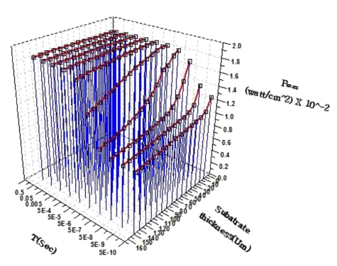
Fig. 2
A 3-dimensional illustration of experimental results: electron recombination lifetime (T) in the x-axis, substrate thickness (10 μm-150 μm) in the y-axis, and maximum cell output power in the z-axis.
The said results contrast significantly to that of a standard front-lit design that was investigated earlier.6) In it, it was shown that both the substrate thickness and the recombination lifetime came into play at all levels and gave a rise to optimum substrate thickness/recombination lifetime combinations that yield maximum power output, i.e., 80 μm or thicker/5 × 10−5 sec or longer to yield 20.2 mW·cm−2, 70 μm/5 × 10−6 sec to yield 20.2 mW·cm−2, 40 μm/5 × 10−7 sec to yield 19.4 mW·cm−2, 20 μm/5 × 10−8 sec to yield 17.5 mW·cm−2, 10 μm/5 × 10−9 sec to yield 13.4 mW·cm−2, and 10 μm/5 × 10−10 sec to yield 6.0 mW ·cm−2. The straight line fit of these data points yielded an approximate equation that is6)(3.1)
where
F(x) ≡ substrate thickness for the maximum power output, μm
x ≡ absolute exponent value of the minoritycarrier recombination lifetime.
The absence of the optimum substrate thickness/recombination lifetime combinations in this study indicate that the BCBJ design calls for an extremely high-quality material that has a long minority-carrier recombination lifetime for its substrate or else an extremely thin substrate.
The significance of a long recombination lifetime or a thin substrate can be understood by visualization as in Fig. 3. In the BCBJ structure as shown, most of the light absorption, or electron-hole pair generation, takes place near the surface of the p-type substrate, very far away from the pn junction, i.e., quite opposite of the front-lit design where most of the light absorption takes place near the pn junction. As such, electrons that are minority carriers in the p-type substrate have nearly the entire thickness of the substrate to travel from the generation sites to the n-type emitter side of the pn junction. To accomplish this feat, the electrons need to have recombination lifetime that is sufficiently long or else the substrate needs to be very thin. In comparison, the minority-carrier recombination is not as much an issue in the front-lit design where the generation sites are not far from the pn junction. In this regard, the present study with BCBJ design shows that the minority-carrier recombination lifetime needs to be at least an order of magnitude longer than that of the front-lit design, i.e., 5 × 10⁻⁴ sec vs. 5 × 10⁻⁵ sec, to achieve the maximum possible power output.
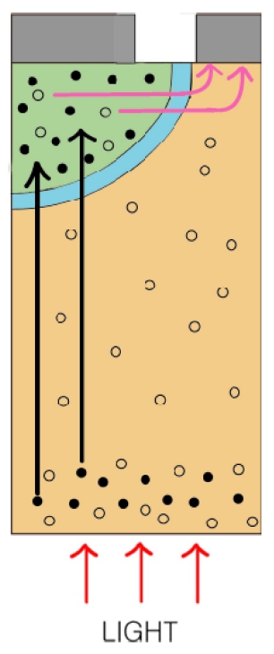
Fig. 3
Minority-carrier movements in the BCBJ design: the electrons (dark circles near the bottom in the p-type substrate) have long distances to travel from the generation sites to the n-type emitter at the top, thus requiring a long recombination lifetime, and the holes (light circles in the n-type emitter) have a shorter distance to travel, but are surrounded by more majority electrons.
As minority-carrier recombination is partly enhanced by crystalline defects and impurities, a longer recombination lifetime requires a purer material. For the standard front-lit solar cells, polycrystalline silicon is widely used for its reduced cost. In view of the results so far discussed, polycrystalline silicon in bulk form may not be an option for the BCBJ solar cells. For it to be viable in the BCBJ application, polycrystalline silicon probably needs to be in the state of thin film.
In short, a BCBJ or back-lit Si solar cell was examined by Medici, a simulation software tool, to determine the effect of the variations in minority-carrier recombination lifetime and substrate thickness on the solar cell power output. For high-quality (long recombination lifetime) substrates, a maximum power output was achieved independent of substrate thickness, while the situation is not quite the same for poor-quality (short recombination lifetime) substrates. In this regard, the critical value of recombination lifetime required for practical BCBJ solar cells is found to be 5 × 10⁻⁴ sec. A lifetime shorter than this value would result in significant loss of the output power.
4. Conclusion
The BCBJ or back-lit solar cell by design has the pn junction and metal contacts all on one side that faces away from the sun. This eliminates the loss by shading completely. However, as the electron-hole generation sites are very far from the pn junction, loss by minoritycarrier recombination can become a significant issue. The interdependency between substrate thickness, which determines the distance between the generation sites and the pn junction, and the minority-carrier recombination lifetime was studied in terms of how they affect the solar cell power output. Medici, a 2-dimensional semiconductor device simulation tool, was used in the study. Qualitatively speaking, the results indicate that a very high quality substrate with a long recombination lifetime of minority carriers, i.e., electrons in p-type substrates, is needed to maintain the maximum power generation. The quantitative value of the recombination lifetime required in the BCBJ or back-lit cell is about an order longer than that in the front-lit cell, i.e., 5 × 10⁻⁴ sec vs. 5 × 10⁻⁵ sec. Regardless of the substrate thickness up to 150 μm, the power output in the BCBJ cell stays nearly at the maximum value of about 1.8 × 10⁻² W·cm−2, or 18 mW·cm−2, as long as the electron recombination lifetime is 5 × 10⁻⁴ s or longer. The output power, however, declines steeply to as low as 10 mW·cm−2 when the electron recombination lifetime becomes significantly shorter than 5 × 10⁻⁴ sec. Substrate thinning is found to be not as effective as in the front-lit case in stemming the decline in the output power. In view of the result, for the BCBJ application, polycrystalline silicon that is widely in use in front-lit solar cells may not be suitable in bulk form and may be viable only in thin-film form.
