

1. Introduction
Recently, organic light emitting diodes (OLEDs) have been extensively used in promising applications, such as mobile phones, laptop computers, monitors, televisions, car displays, light sources, and public displays.1,2) OLEDs have emerged as excellent candidates for next-generation displays, having progressively replaced liquid crystal displays (LCDs) in high-resolution display systems, because OLEDs have self-luminous pixels that overcome the disadvantage of LCDs, which have thick, heavy, back light units (BLUs). OLEDS are thinner and have lighter weight, a wider viewing angle, and a much higher contrast ratio in comparison with LCDs.3,4) Much research has been focused on optimizing thin-film transistors (TFTs) based on semiconductor materials as a way to enhance the performances of large-size OLEDs.5,6) Among the various amorphous-oxide materials, amorphous In-Ga-Zn-O (a-IGZO) thin films have been predominantly considered due to their having significant advantages, such as compatibility with the amorphous silicon process in large-area mass production, high mobility, and both short- and long-range uniformity.7,8) Demands for high-performance, high-resolution, and large-size OLEDs have been dramatically increasing with increasing requirements for high-quality image density. Although several inherent problems limit the ability to achieve ultrahigh image density from a large-size OLED, if such an image density were to be achieved using a large-size OLED, that would play an important role in making large-size display systems more practical.9)
Amorphous silicon TFTs (a-Si TFTs) with a high uniformity have been extensively utilized in the fabrication of large-size LCDs. However, the low mobility and the large threshold voltage (Vth) shift of a-Si TFTs make their use as reliable backplanes for OLEDs difficult.10) Low-temperature poly-silicon (LTPS) TFTs, which have superior characteristics including high mobility and high stability, are currently being used for small size OLEDs.11) However, the use of LTPS TFTs with poor uniformity in large-size OLEDs is difficult unless an additional complicated compensation pixel is included, but the inclusion of such a pixel would decrease the yield rate of mass production.12) To the contrary, IGZO TFTs can be conveniently manufactured using the existing amorphous Si TFT process line. Even though some investigations on the device performances of conventional TFTs used in displays have been conducted,13,14,15,16) studies on the achievement of ultra-high-definition (UHD) large-size OLEDs containing a-IGZO TFTs with a coplanar structure have not yet been performed. This paper presents data demonstrating the achievement of an UHD from large-size OLEDs based on a-IGZO TFTs with a coplanar structure. The a-IGZO TFTs with a coplanar were fabricated so as to enhance their uniformity and reliability.17) Drain currents were measured as functions of the gate voltages for the a-IGZO TFTs to investigate the uniformity of their threshold voltages. Drain currents were also measured as functions of the drain voltages to investigate the saturation characteristics of the currents for the TFTs. Moreover, the drain currents for TFTs that had been subjected to a voltage bias or a current stress were measured as functions of the gate voltages to investigate their current fluctuations and stabilities. Finally, the performance of large-size OLEDs embedded with TFTs with a coplanar structure in producing UHD was investigated.
2. Experimental Procedure
The detailed structure of the etch-stopper-layer (ESL)-type TFTs with a double gate formed by placing gates on the top and the bottom regions of the active layer is described elsewhere.18) The ESL is necessary to protect the active film against the introduction of contaminants, which might deteriorate the reliability of oxide TFTs, so that a TFT with high performance can be achieved.19,20,21,22,23)
In this study, in order to prevent contamination of the active channel during the coplanar TFT process, gate insulation (GI) and gate metal were continuously deposited using a top gate structure and a self-aligned method, and the gate and GI layers were patterned simultaneously. As a result, it was possible to prevent channel contamination during source-drain patterning. The TFTs with the ESL structure generate large parasitic capacitances between the gates and the drain/source metals. Those large parasitic capacitances induce the signal RC delay and decreases the operating speed of the driving circuit of the display panel. TFTs with a coplanar structure were fabricated to overcome the drawbacks of the ESL type TFTs and to satisfy image-density requirements for potential applications in large-size OLEDs.
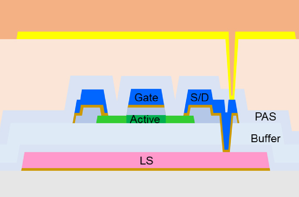
A cross-sectional view of such a self-aligned thin-film transistor with a coplanar structure containing a top gate is shown in Fig. 1. Novel technologies that were adopted for use in this fabrication process included the fabrication of top gate TFTs without overlap between metals, selective metallization of the active layer in the source/drain regions, and the formation of a light shield layer. First, a 35 nm thick active layer of the a-IGZO film was formed by using a direct-current sputtering method, after which it was patterned by using a wet-etching method. A 180 nm thick gate dielectric material was formed by using plasma-enhanced chemical-vapor deposition, followed by the growth of a bilayer of MoTi and Cu as a 400 nm thick gate and S/D electrode. After the gate electrode had been etched in a wet-bath, the gate insulator was dry-etched by using a photoresist of the gate pattern. The concentration of oxygen vacancies in the plasma-treated area was much larger than that in the non-treated area. Oxygen vacancies were easily generated near the surface of the a-IGZO region due to the plasma treatment and were later filled with oxygen from the environment during annealing or the formation of the SiO2 layer. The plasma-treated a-IGZO surface on the source/drain region was formed by using dry etching. The sheet resistance of the a-IGZO on the source/drain region was decreased. The parasitic capacitance of the TFT was dramatically reduced by adopting a top gate TFT and a self-aligned conductive active layer in the source and drain regions.24) TFTs with a highly conductive a-IGZO film are necessary if the contact resistance is to be reduced and the current flow enhanced.25,26) Because the superfluous capacitance of the TFTs interrupts the effective operation of large-size OLEDs and has an adverse impact on their performance, a coplanar structure and an optimized heat process were adapted to improve the reliability of the TFTs.27,28)
The reliability of the values of the Vth for the TFTs was characterized by using both an in-line probe station and an automatic sensing method. Test element groups (TEGs) with transistors at many sites on the glass substrates were monitored by using an in-line probe station. Additionally, the values of the Vth were determined for the TFTs for all pixels inside the UHD panel by using a real-time automatic Vth sensing method.
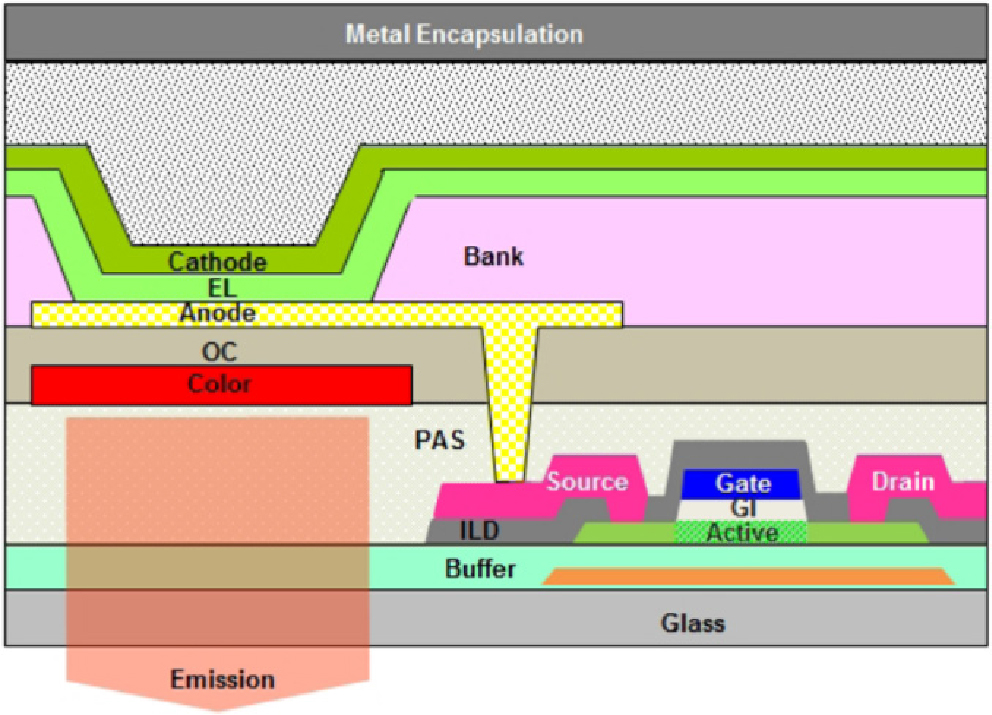
Fig. 2 shows a cross-sectional view of a large-size OLED embedded with coplanar oxide TFTs fabricated on a 2,500 × 2,200 mm2 glass substrate. The large-size OLED fabricated on 0.5 t glass, which acts as a bottom emission-type display, consists of coplanar-type TFTs, a white OLED (WOLED) with white, red, green, and blue color layers, and the metal encapsulation. Because the emission region of an OLED increases with decreasing size of the TFT, a coplanar TFT with a smaller size would be useful if promising applications in large size OLEDs are to be realized.
3. Results and Discussion
In a self-aligned thin-film transistor with a coplanar structure, the active layers in the coplanar TFTs, except for the gate mask, were exposed to plasma treatments, resulting in the formation of a highly conductive region. The results from Rutherford backscattering spectrometry performed on the plasma-treated active layer demonstrated that the amount of oxygen at the surface of the active layer was larger than that in the bulk. The detailed results of the Rutherford backscattering spectrometry measurements on the plasma-treated active layer in the coplanar TFTs are described elsewhere.29) Unlike TFTs with a bottom gate structure, the TFTs with a top gate structure were exposed to light that had been transmitted through the glass substrate. The light shield layer was moderately designed to reduce the negative bias temperature illumination stress. The drain current of the TFTs was observed to increase due to a decrease in the drain-induced barrier lowering. Moreover, coplanar TFTs capped with a light shield layer are considered to be superior candidates for use as TFTs with a backplane structure for enhancing the image density of OLEDs. While the reliability of the TFTs with an ESL structure is better than that of the TFTs with a coplanar structure, which is due to the existence of the ESL protecting the active channel layer,30) the parasitic capacitance of the TFTs with an ESL structure is larger than that of the TFTs with a coplanar structure due to the existence of the overlapping area. Furthermore, the photomask number of the coplanar TFTs is smaller than that of the ESLtype TFTs, resulting in a simpler process.
Fig. 3 shows that the transfer curve of the fabricated TFT, average value of Vth is 0.10 V, and the difference between the maximum and the minimum values of the Vth for a TFT fabricated on a 2,500 mm × 2,200 mm glass, were 0.57 and 0.55 V as determined by using the in-line probe station and the automatic Vth sensing method, respectively. This improvement in the uniformity of the Vth for the coplanar TFTs, as compared to that of the ESL TFTs, was achieved via the optimization process.
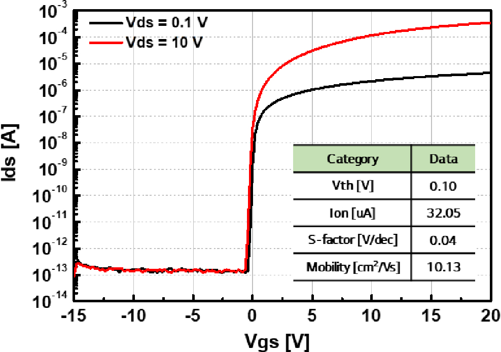
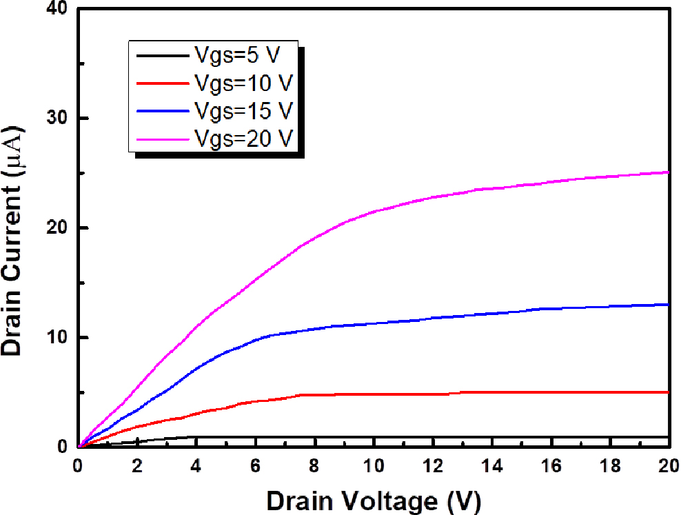
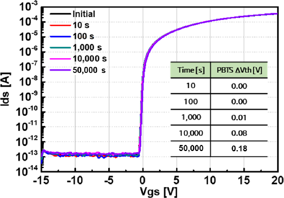
Fig. 4 shows the drain current as a function of the drain-source voltage (Vds) for various values of the gate-source (Vgs) voltage ranging from 5 to 20 V. The variation in the output drain current for the TFTs at Vds = 10 V can be characterized by using the differential dIds/dVds. The value of that differential in the saturation region for coplanar TFTs with a light shield is almost the same as its value in that region for etch stopper TFTs, indicating that the output current of the OLEDs is not significantly affected by variations in the drain-source voltage. The shifts in the values of Vth for the TFTs were measured under a positive bias temperature stress (PBTS) and under a current stress (CS). Both of these electrical stresses were applied to the TFTs at 60 °С using Vgs = + 30 V, Vds = 0 V, and a constant current.
The shift in the value of Vth under the PBTS was 0.18 V after 50,000 s, as shown in Fig. 5. Because the device characteristics of coplanar TFTs vary only slightly during long-time operation, under applied voltages, and exposure to environmental temperatures, such TFTs can be used in large-size OLEDs. The uniformity of the current applied to the TFTs in OLEDs is particularly important if reliable outputs from the OLEDs are to be achieved.
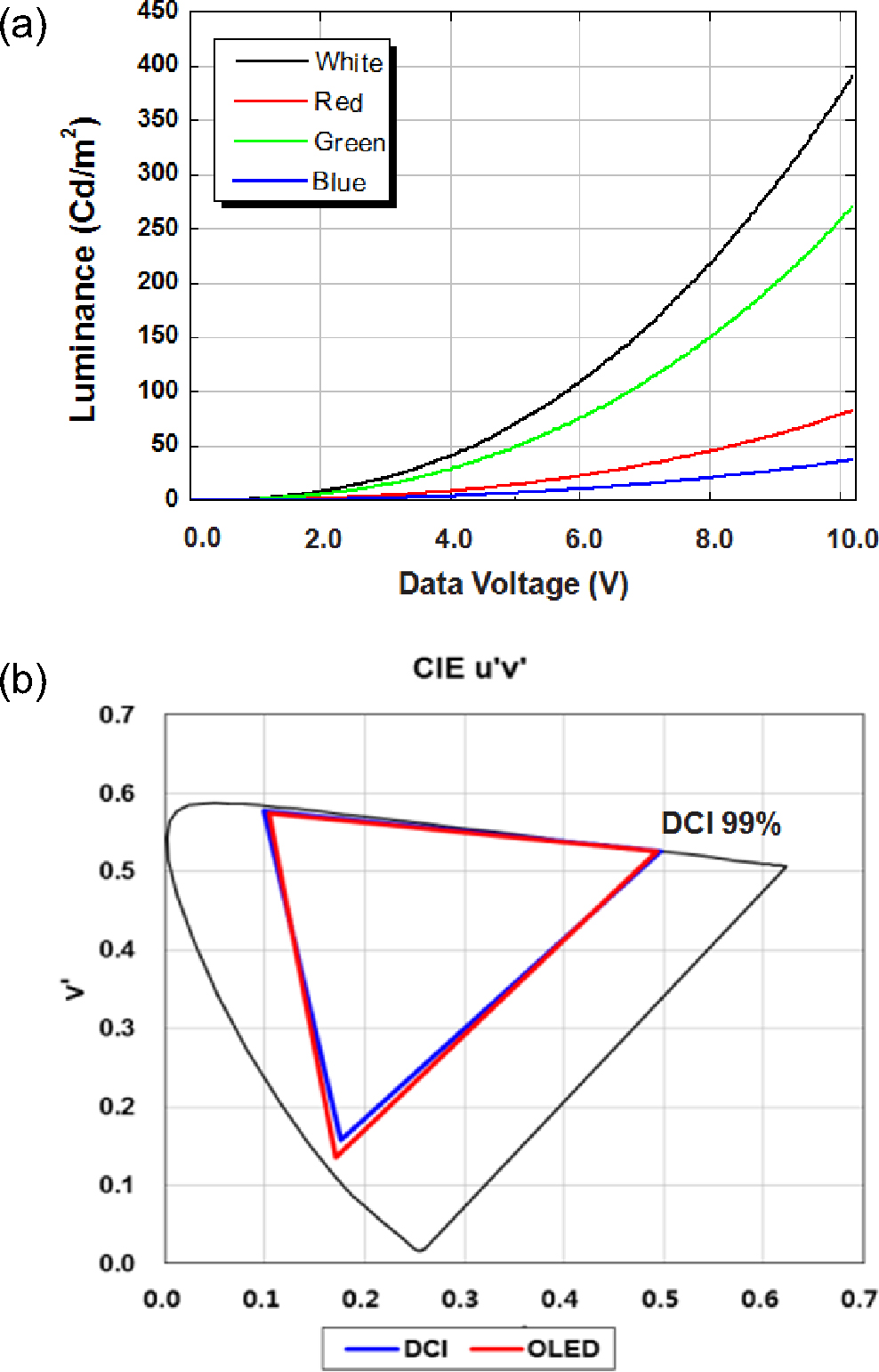
The characteristics of the white OLEDs are summarized in Table 1. The luminance efficiency of the OLEDs at an operating voltage of 11.6 V was 85.0 cd/A. The Commission Internationale de l’Eclairage (CIE) coordinates of the OLEDs are (0.287, 0.310), indicative of a white color, and the dependence of the color shift on the area is only 0.011. The device characteristics of a 77-inch UHD OLED embedded with TFTs with a coplanar structure for practical mass production are summarized in Table 2. One pixel was designed to contain one white, one red, one green, and one blue sub-pixel and to have an average aperture ratio of 30 % and a peak luminance of 500 cd/m2, thus demonstrating the achievement of an UHD large-size OLED. Although a 77-inch full high-definition OLED panel can be designed using conventional TFTs, 77-inch ultra-high-definition (UHD) panels cannot, which is the reason TFTs with a coplanar structure should be used for the fabrication of UHD large-size OLEDs. Fig. 6(a) shows that the maximum luminance of the large-size OLED is 500 nits, indicative of a UHD large-size OLED. As Fig. 6(b) shows, the color gamut of the fabricated OLED satisfies the requirements of the digital cinema initiatives (DCI) of 99 %.
Table 1.
Characteristics of the fabricated OLEDs.
| Item (unit) | Content |
| Voltage (V) | 11.6 |
| Efficiency (cd/A) | 85.0 |
| Color (Wx, Wy) | (0.287, 0.310) |
| Color shift (delta u’v’) | 0.011 |
4. Conclusion
The top gate, the self-aligned metallization of the active layer as in the source/drain regions, and the light shield layer of the TFTs were selected so as to enhance the image density of the OLEDs. The a-IGZO oxide TFTs with a coplanar structure on glass substrates showed maximum Vth differences of 0.57 V in the TEG transistors and of 0.55 V in the active-area transistors, indicative of their excellent uniformity. The values of the Vth for the TFTs with a coplanar structure after having applied a PBTS for 50,000 s were slightly shifted to 0.18 V, indicative of their stability. The maximum luminance of the OLEDs embedded with TFTs with a coplanar structure was as large as 500 nits, and their color gamut exhibited a DCI of 99 %, indicative of the achievement of large-size UHD OLEDs. The CIE coordinates of the OLEDs were (0.287, 0.310), indicative of a white color, and the dependence of the color shift on the area was only 0.011. Moreover, the luminance efficiency of the white OLEDs embedded with TFTs with a coplanar structure at an operating voltage of 11.6 V was 85.0 cd/A. Thus, the present observations provide good motivation for envisioning the use of UHD large-size OLEDs embedded with TFTs with a coplanar structure in UHD large-size OLED televisions.
